Appendix A
-
137
-
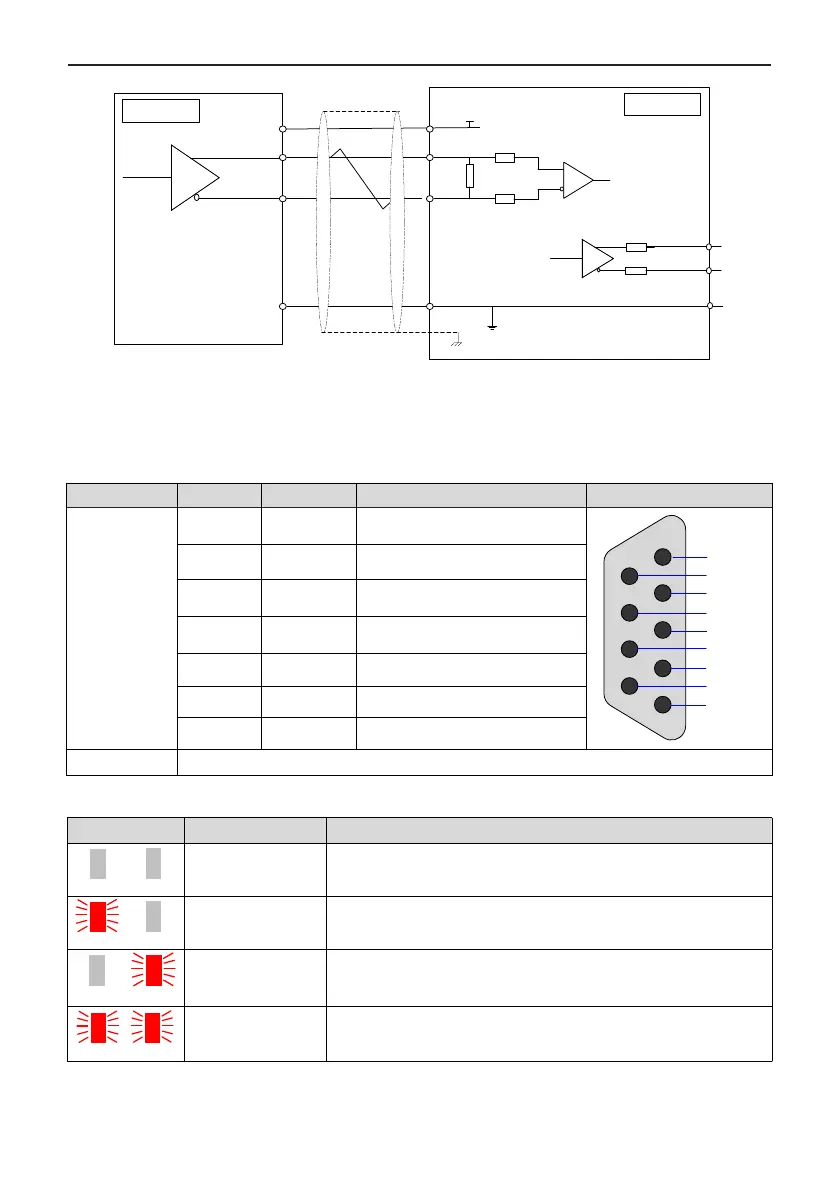
Shield
26C31
26C
32
5V
COM
A+,B+,Z+
A-,B-,
Z-
COM
Frequency
dividing output
PG card
VCC
0V
A+
,B+,Z+
A-,B-,Z-
A+,B+,Z+
A-,B-,Z-
PE
Twisted
pair
Encoder
Figure A-5 Port circuit of MD38PG1
A.5.4 Resolver PG Card (MD38PG4)
Table A-12 Terminal descriptions of MD38PG4
Terminal Pin Denition Function Description Terminal Arrangement
J3
1 EXC1 Resolver excitation negative
1
2
3
4
5
6
7
8
9
EXC1
EXC
NC
NC
SIN
NC
SINLO
COSLO
COS
2 EXC Resolver excitation positive
3 SIN Resolver feedback SIN positive
4 SINLO Resolver feedback SIN negative
5 COS Resolver feedback COS positive
6, 7, 8 NC Vacant internally
9 COSLO Resolver feedback COS negative
CN1 18-pin FFC interface, connecting to J4 on the control board of the AC drive
Table A-13 Indicators of MD38PG4
Indicator State MD38PG4 Fault State Description
Normal None
Phase-lock loop
unlocked
Phase lag of the resolver is very large.
Signal SIN/COS
amplitude exceeding
the upper limit
D6 ashing is normally caused by interference. Ground the motor well and
connect the ground point of the resolver card to PE of the drive.
Signal SIN/COS
amplitude too small
Generally, DB9 is not connected or wrongly connected, or even wire
breaks. If the preceding conditions do not occur, check whether the resolver
model selection is correct or not.
 Loading...