P/N 960-000180R_Rev. 1 {EDP #233427} © 2016, JAPAN CASH MACHINE CO., LTD.
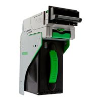
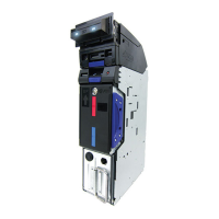
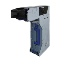
Section 2 DBV® Series DBV-400 Banknote Validator Installation
Standard Interface Circuit Schematics (Continued 1)
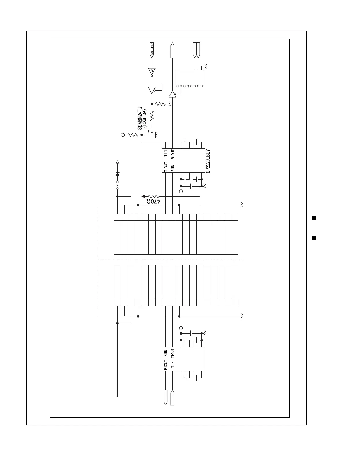
Figure 2-12 illustrates the DBV-400 ID-003 RS232C Interface Schematic Diagram.
Figure 2-12 DBV-400 ID-003 RS232C Interface Schematic Diagram
Figure 2-12 DBV-400 ID-003 RS232C Interface Schematic Diagram
1
2
3
4
5
6
7
8
9
10
11
12
13
14
15
16
17
18
1
2
3
4
5
6
7
8
9
10
11
12
13
14
15
16
17
18
IN12V-24V
GND
IN12V-24V
GND
RxD
GND
IN12V-24V
GND
IN12V-24V
GND
TxD
TxD
GND
Power
3.3V
5V
Power 3.3V
22K
Sleep Control
INLINE1
IFSEL1
IFSEL2
(Exar)
Y0
Y1
Y2
Y3
Y4
Y5
Y6
Y7
A
B
C
RxD
CONTROLLER SIDE
DBV-400 SIDE