Page 7.3 - 42 COMBIVERT F5-A, -E, -H © KEB, 2012-10
Digital in- and outputs
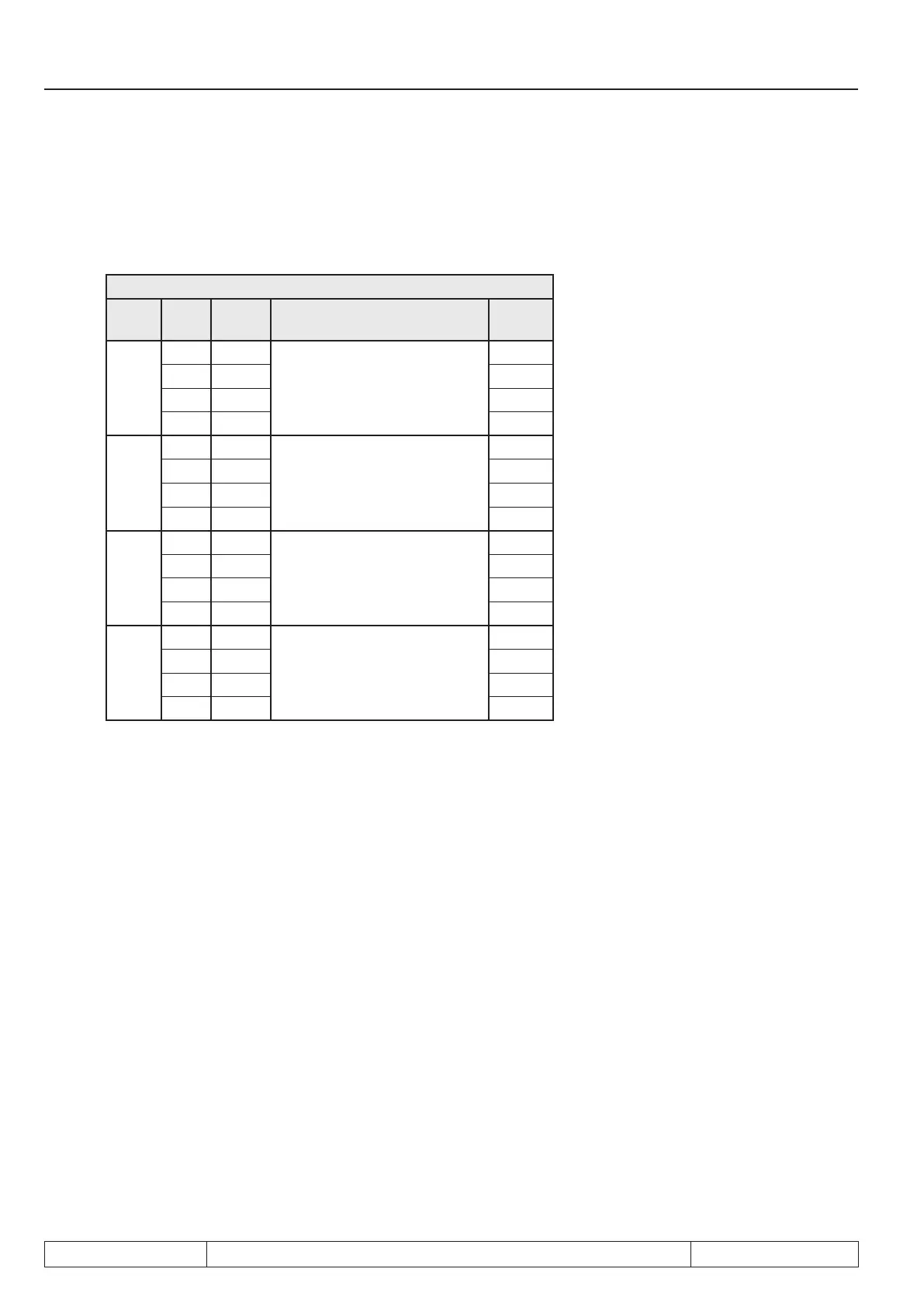
7.3.25 Hardware output allocation (do.51)
The output signals are allocated to output terminals O1, O2, R1 and R2 with do.51. The assignment is done
according to following table:
do.51:Hardware output allocation
Bit Va-
lue
Signal output Default
0 + 1
0 O1
O1 (terminal X2A.18)
x
1 O2
2 R1
3 R2
2+3
0 O1
O2 (terminal X2A.19)
4 O2 x
8 R1
12 R2
4+5
0 O1
R1 (terminal X2A.24...26)
16 O2
32 R1 x
48 R2
6+7
0 O1
R2 (terminal X2A.27...29)
64 O2
128 R1
192 R2 x
7.3.26 Programming example
For a better understanding, the correlations are explained on the basis of a more complex example. Following
conditions are required:
• Condition 1: Output X2A.19 switches, if the inverter accelerates
• Condition 2: Relais X2A.24...26 switches, if the inverter load is > 100 %
• Condition 3: Relay X2A.27...29
• Output X2A.18 switches, if the conditions 2 and 3 are realized, but the inverter does not accelerate.
Solution proposal:
Adjust switching conditions, levels and hysteresis
First adjust the switching conditions and levels.
do.00 to „21“ (inverter accelerates),
do.01 to „24“ (inverter utilization > level); LE.01 to „100“ (load level for do.01 100 %); LE.09 to „5“ (5 % hystere-
sis for comparison level 1; not required but reasonable for optimal switching performance),
do.02 to „27“ (actual value > level); LE.02 to „4“ (frequency level for do.02); LE.10 to „0.5“ (0.5 Hz hysteresis for
comparison level 2; not required but reasonable for optimal switching performance).
 Loading...