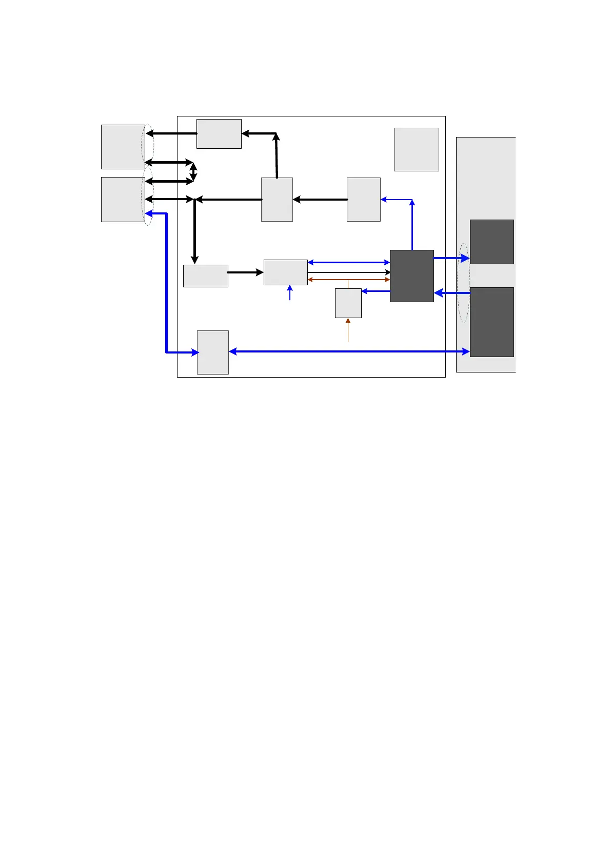
4-6 Product Principle
4.3 TR64 Board
Main board
TRA
FPGA
Signal
process
FPGA
TR64 board
High-
voltage
pulse
output
circuit
Drive
circuit
High-
voltage
isolation
AFE clip
x8
Clock offered
by CPU
TRB
FPGA
Clock
circuit
65-128
RX,
64ch
64ch
64ch
CPU ATGC
Pencil
probe
transmitting
switch
Control
Data
Probe
board
Main
board
1-64
CW
transmitting
power
supply
Probe
control
SPI
TX,64ch
Transmitting
control
PEN_TX
C
T
B
C
T
B
C
T
B
Control signal
65-128
Fig
4-5 Principle diagram of TR64 board
The main functions of TR64 board:
Control FPGA (TRB, implements the control of 1-64 channels transmitting and receiving,
ATGC adjustment and CW receiving control).
Clock circuit provides the clock for transmitting/receiving chip.
Transmitting circuit (transmits the pulse with the achievement of 5 electric levels and CW)
High-voltage isolation
AFE (receives echo signal)
ATGC circuit (time gain compensation)
Probe port function (Probe recognition signal, power supply control of the probe)
4.4 Probe Board
Supports 192/128 array probe, phased array probe, bi-plane probe, and other nominal
probes, etc.
Implements the connection between the main unit and the probe.