Circuit Descriptions, Abbreviation List, and IC Data Sheets
EN 157BJ3.0E PA 9.
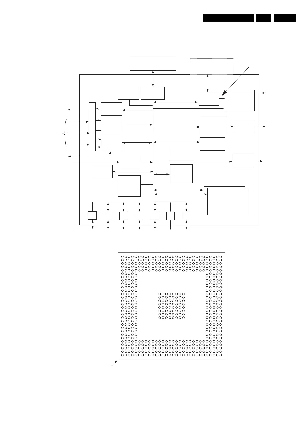
9.11.8 Diagram B5x, PNX8550EH (IC 7V00)
Figure 9-17 Internal block diagram and pin configuration
E_14700_088.eps
250505
Block Diagram
Pin Configuration
TS Out
1SD+1HD
YUV422
Video In
Dual
Cond.
Access
20
Dual SD
Single HD
MPEG2
Decoder
re
tuoR ST
/oed
iV
Audio In
Audio Out
250 MHz
MIPS32
CPU
2x 240 MHz
TM3260
Media Processor
2D DE
Temporal
Noise Redux
DVD-CSS
5-Layer
Primary
Video Out
HD/VGA/656
2-Layer
Secondary
Video Out
3x656
30 (dig)
Analog
MemoryStick/
MultiMedia Card
2x Smartcard
UARTs
USB1.1
GPIO
PCI2.2
2x I2S
SPDIF
2x I2S
SPDIF
PNX8550
32-Bit 225 MHz DDR
10
Flash IDE
S-Video or
CVBS
Tunnel
Optional External
Video Improvement
Processing
DENC
Memory
Controller
TS Output
TS Inputs
Streaming Interface
from Tunnel
De-interlacer
Scaler and
A
B
C
D
E
F
H
K
G
J
L
M
N
P
R
T
U
V
W
Y
AB
AD
AH
AK
AF
AA
AC
AJ
AG
AE
2 4 6 8 10 12 14 16 18 20 22 24 26 28 30
135791113 2115 17 19 23 25 27 29
shape
optional (4x)