PG-FP5 CHAPTER 10 NOTES ON TARGET SYSTEM DESIGN
R20UT0008EJ0400 Rev. 4.00 Page 193 of 240
Jul 15, 2010
(3/3)
Target Device Pin Recommended Design
I/O pins
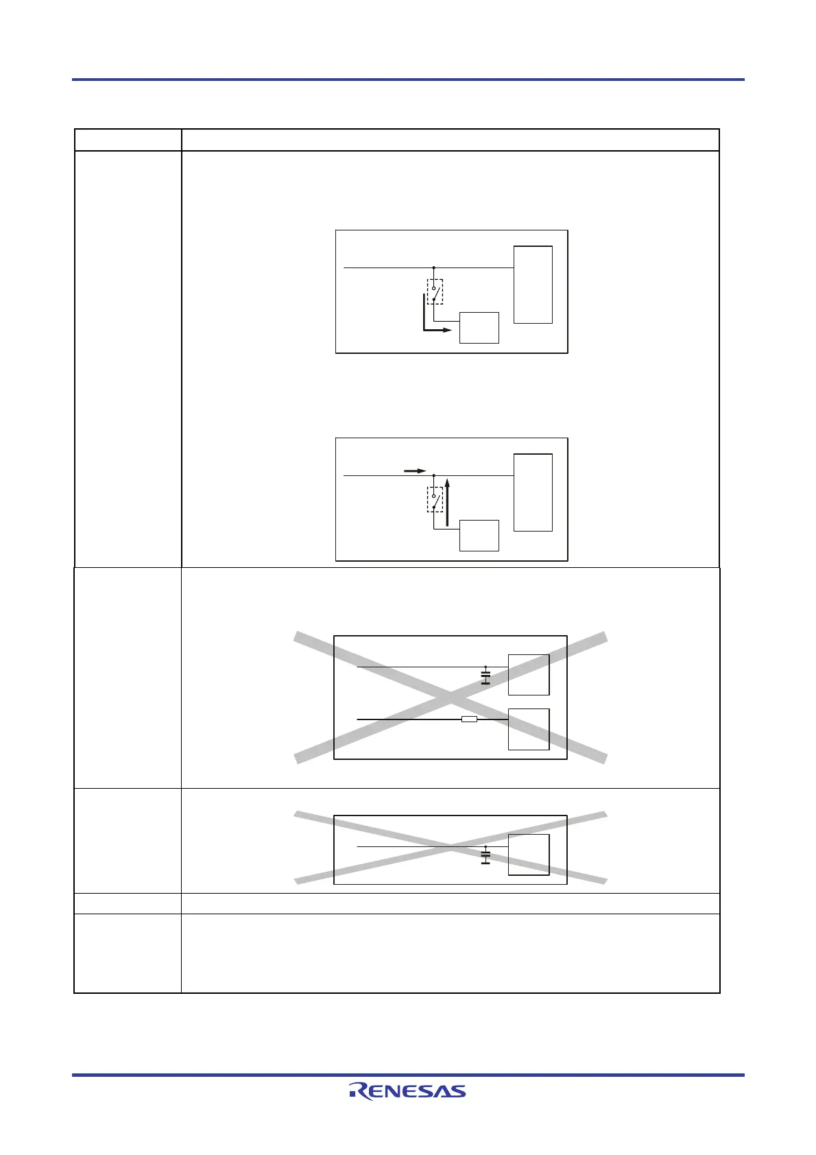
When a target device pin used by the FP5 is also connected to the input of an external device, and if that
target device malfunctions, disconnect the external device as shown in the portion below enclosed in the
dotted line or make it output high impedance like dotted line.
Example:
Adverse effect
FP5 input pin
Input
External device
SO/TxD
Target device
If a target device pin used by the FP5 is also connected to the output of an external device like dotted line,
and a signal collision occurs, disconnect the external device as shown in the portion below enclosed in the
dotted line.
Example:
Conflict
FP5 output pin
Output
External device
SI/RxD
Target device
VPP Keep the wiring between the FP5 connector and the target device VPP pin as thick and as short as possible.
Insert neither capacitors nor resistors into the VPP line unless otherwise stated.
Incorrect circuit:
VPP
FP5 VPP
FP5 VPP
VPP
Target device
Target device
FLMD0 Insert neither capacitors nor resistors into the FLMD0 line unless otherwise stated.
Target device
FLMD0
FP5 FLML0
FLMD1 Connect the FP5, or GND using pull-down resistance on board.
Others For the recommended connection of unused pins, refer to the user’s manual of the target device.
Some target devices have pins that must be connected differently. For these pins also, refer to the user’s
manual of the target device.
Example of pins connected differently: MODE, CKSEL, REGOUT, REGIN, etc.