Publication 1769-UM002B-EN-P - July 2005
Overview 1-7
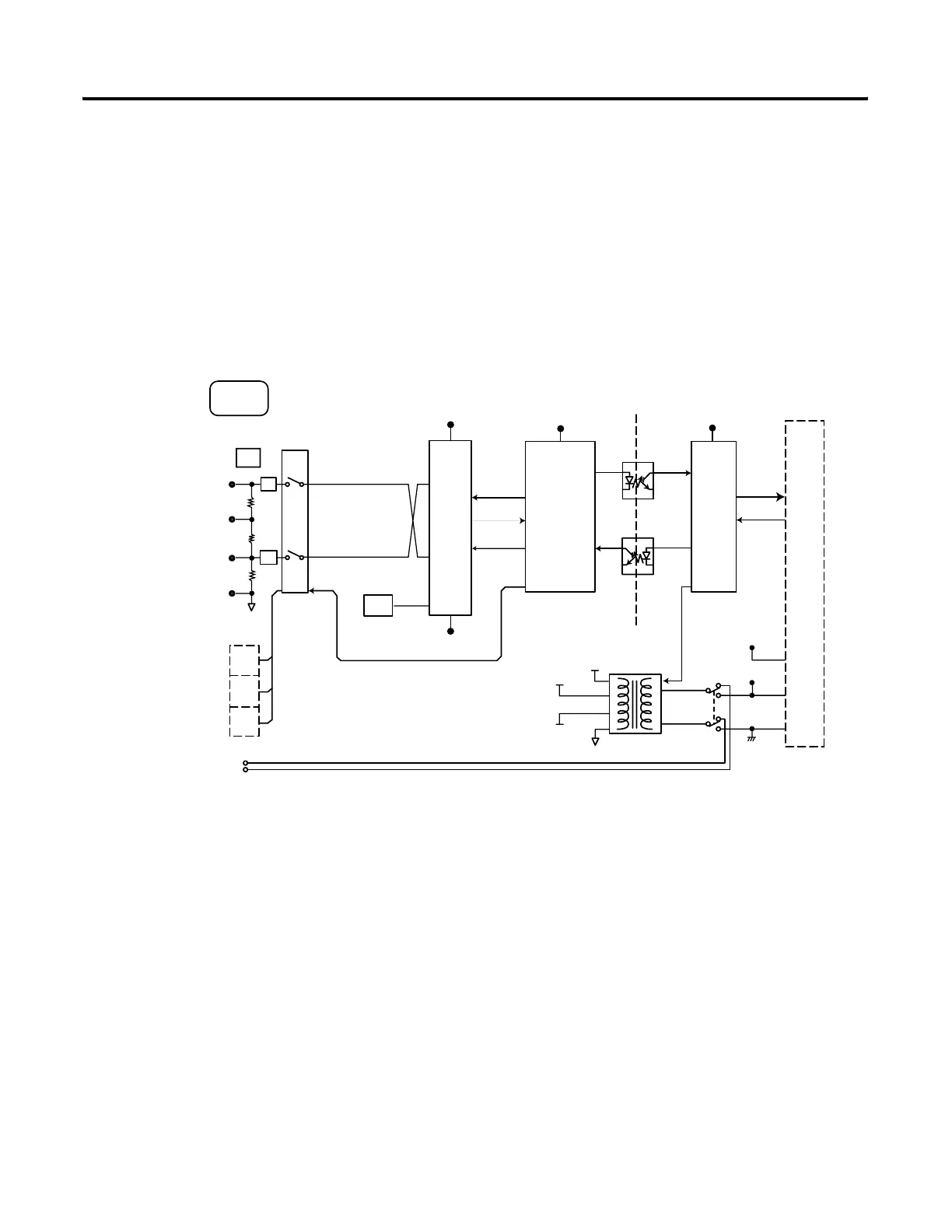
Module Operation
Input Module Block Diagram
The input module’s input circuitry consists of four differential analog inputs
multiplexed into a single analog-to-digital (A/D) converter. The
A/D converter reads the selected input signal and converts it to a digital value
which is presented to the controller. The multiplexer sequentially switches
each input channel to the module’s A/D converter.
Figure 1.5 1769-IF4 Block Diagram
Vin+
Iin+
V/Iin-
COM
+24V dc
dc Neutral
CH0
CH1
CH2
CH3
A-GND
Vref VREF
AIN-
AIN+
A/D
MCU ASIC
VA3
VA2
VA2
VA1
VA3
VA1 VS1
VS1
VS2
TXD
RXD
A-GND S-GND
Input
(same as above)
Channel Select
DC/DC
Power
Supply
Galvanic
Isolation
Multiplexer
Bus
 Loading...