STR-DA2800ES
STR-DA2800ES
5656
For Schematic Diagrams.
Note:
• All capacitors are in μF unless otherwise noted. (p: pF) 50
WV or less are not indicated except for electrolytics and
tantalums.
• All resistors are in Ω and 1/4 W or less unless otherwise
specifi ed.
•
f
: Internal component.
• 2 : Nonfl ammable resistor.
• 5 : Fusible resistor.
• C : Panel designation.
THIS NOTE IS COMMON FOR PRINTED WIRING BOARDS AND SCHEMATIC DIAGRAMS.
(In addition to this, the necessary note is printed in each block.)
• A : B+ Line.
• B : B– Line.
• Voltages and waveforms are dc with respect to ground
under no-signal (detuned) conditions.
no mark
: TUNER
*
: Impossible to measure
• Voltages are taken with VOM (Input impedance 10 M).
Voltage variations may be noted due to normal production
tolerances.
• Waveforms are taken with a oscilloscope.
Voltage variations may be noted due to normal production
tolerances.
• Circled numbers refer to waveforms.
• Signal path.
F : AUDIO
f : TUNER
d : USB
G : C4
N : MIC
E : VIDEO
For Printed Wiring Boards.
Note:
• X : Parts extracted from the component side.
• Y : Parts extracted from the conductor side.
•
f
: Internal component.
• : Pattern from the side which enables seeing.
(The other layers’ patterns are not indicated.)
• Lead layouts
surface
CSP (Chip Size Package) Lead layout of conventional IC
Caution:
Pattern face side:
(Conductor Side)
Parts face side:
(Component Side)
Parts on the pattern face side seen
from the pattern face are indicated.
Parts on the parts face side seen from
the parts face are indicated.
• D-VIDEO, NETWORK and SUB D-VIDEO boards are
multi-layer printed board. However, the patterns of inter-
mediate layers have not been included in diagrams.
• Indication of transistor.
C
B
These are omitted.
E
Q
CEB
These are omitted.
* Replacement of IC106, IC107, IC206 and IC207 on
the NETWORK board used in this unit requires a spe-
cial tool.
* Replacement of IC3505 and IC3506 on the D-VIDEO
board used in this unit requires a special tool.
• The voltage and waveform of CSP (chip size package)
cannot be measured, because its lead layout is different
from that of conventional IC.
Caution:
Pattern face side:
(SIDE B)
Parts face side:
(SIDE A)
Parts on the pattern face side seen
from the pattern face are indicated.
Parts on the parts face side seen from
the parts face are indicated.
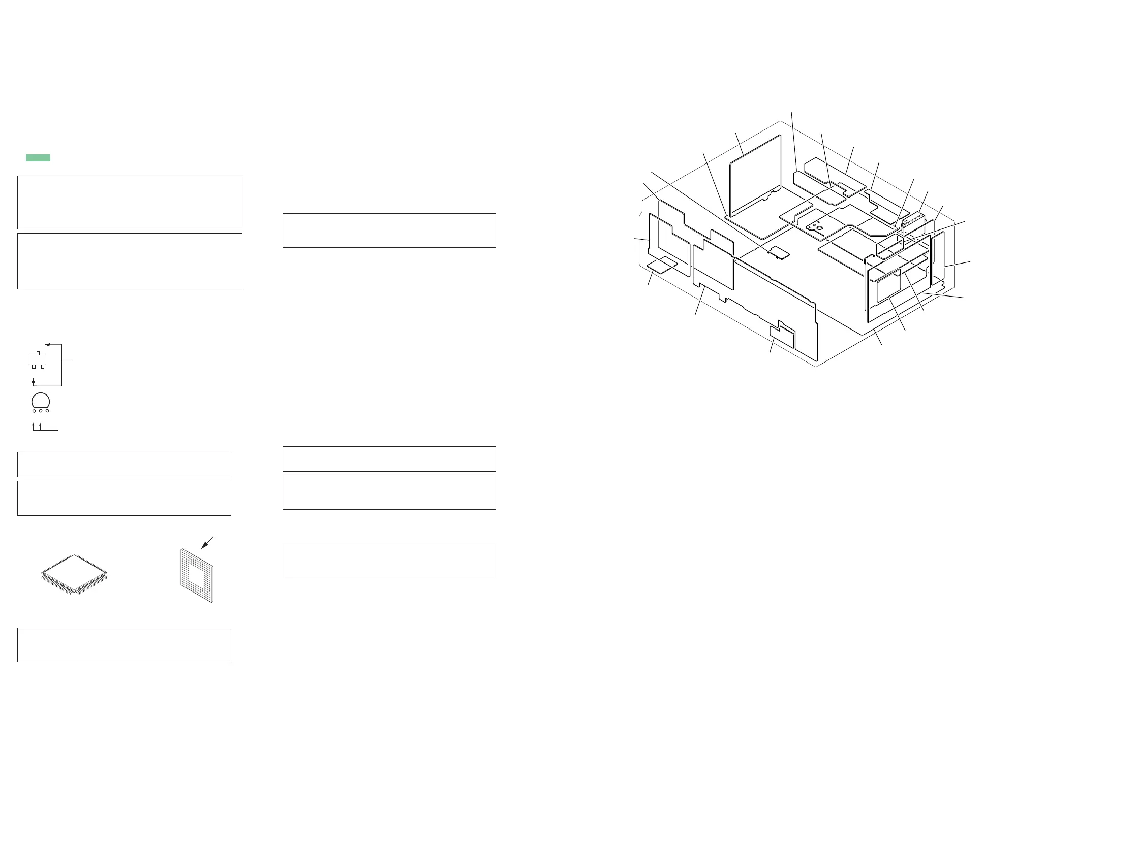
• Circuit Boards Location
* Replacement of IC106, IC107, IC206 and IC207 on
the NETWORK board used in this unit requires a spe-
cial tool.
* Replacement of IC3505 and IC3506 on the D-VIDEO
board used in this unit requires a special tool.
Note: The components identifi ed by mark 0 or dotted
line with mark 0 are critical for safety.
Replace only with part number specifi ed.
Note:
When replacing the complete NETWORK board, refer
to “NOTE OF REPLACING THE COMPLETE NET-
WORK BOARD” (page 6).
Note:
When replacing the complete NETWORK board, refer
to “NOTE OF REPLACING THE COMPLETE NET-
WORK BOARD” (page 6).
TEMP_SENSOR board
POWERKEY board
ACDC board
STBY board
DCDC board
A-VIDEO board
D-VIDEO board
NETWORK board
SURR SPEAKER board
CONTROL board
OPT-COAX board
SUB D-VIDEO board
TUNER (FM/AM) (TU1)
D-AUDIO board
D-AUDIO_CONNECT board
DSP board
HP board
MAIN board
DISPLAY board
USB board
HAT board