• AC1, AC2, BOOT1, and BOOT2 generate noise. Using shielding near these traces (by placing ground
planes below) is recommended.
• Power ground carries the sum of ripple current and DC current from the inverter. Current return paths from
LDO capacitors should be routed separately from these high current paths.
• AC1 and AC2 tracks should be routed close together to minimize the area of the resulting loop.
• Communication (I2C) and sensing signals should be routed far from noise generating nets (AC1, AC2,
BOOT1, and BOOT2) to minimize the effects of interference induced from those high di/dt nets.
• BOOT1, BOOT2 capacitors should be placed as close to the device as possible.
• Input and inverter decoupling capacitors should be placed close to the device to minimize the area of high
current loops.
• Auxiliary LDO capacitors should be placed as close to the device as possible.
• Thermal performance and grounding can be enhanced by dedicating one layer as a ground plane. No
signal/power tracks should be routed on this layer to ensure ground integrity.
6.4 Reference code with STM32 development boards
6.4.1 Hardware requirements
1. STM32 development board (for example, STM32 Nucleo-144)
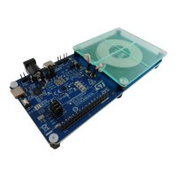
2. STEVAL-WBC86TX
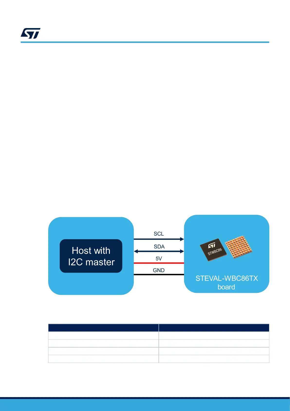
6.4.2 Hardware connections
1. Connect the STWBC86’s I2C pins to the master I2C bus. These signals require pull-up resistors to work
properly.
2. Power up STWBC86.
Figure 67. Pin connection between host and STWBC86 chip/evaluation board
STM32 Nucleo-144 board is used as an example.
Table 7. Pin connection between host (STM32) and STWBC86
STM32 Nucleo-144
STEVAL-WBC86TX board
5V (CN11.18) VIN
GND (CN11.20) GND
I2C1_SDA (PB9 -> CN12.5) SDA
I2C1_SCL (PB8 -> CN12.3) SCL
UM3161
Reference code with STM32 development boards
UM3161 - Rev 1
page 52/78