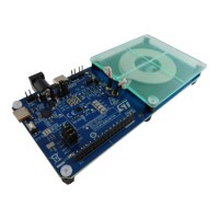
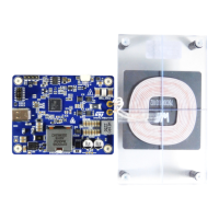
Table 2. Connectors and test points
Connector / test point Name Description
VIN VIN Input voltage (power pins)
VINV VINV Inverter voltage pins
P2 I2C SDA, SCL, INT, and RST signals for I2C communication
P14 Digital interface I2C, GPIO, and RST signals
TP1 Ring node Ring node
TP2 VIN STWBC86 input voltage sensing
TP3 AC2 Resonant circuit terminal
TP4 AC1 Resonant circuit terminal
TP5 VINV STWBC86 inverter voltage sensing
TP6 V1V8 STWBC86’s 1.8 V LDO output
TP7 GND Ground
TP8 VS VS signal sensing
2.2 Basic operating modes
The STWBC86 is designed to work in transmitter mode only. Once the board is powered up, the device
automatically starts pinging (if enabled), which means it starts scanning its power transfer interface for a potential
power receiver. Once a suitable receiver is found, the STWBC86 initializes power transfer. After the receiver is
removed from the interface, the device returns to the pinging phase.
UM3161
Basic operating modes
UM3161 - Rev 1
page 6/78