Aligna
®
4D User Manual
10 / 84
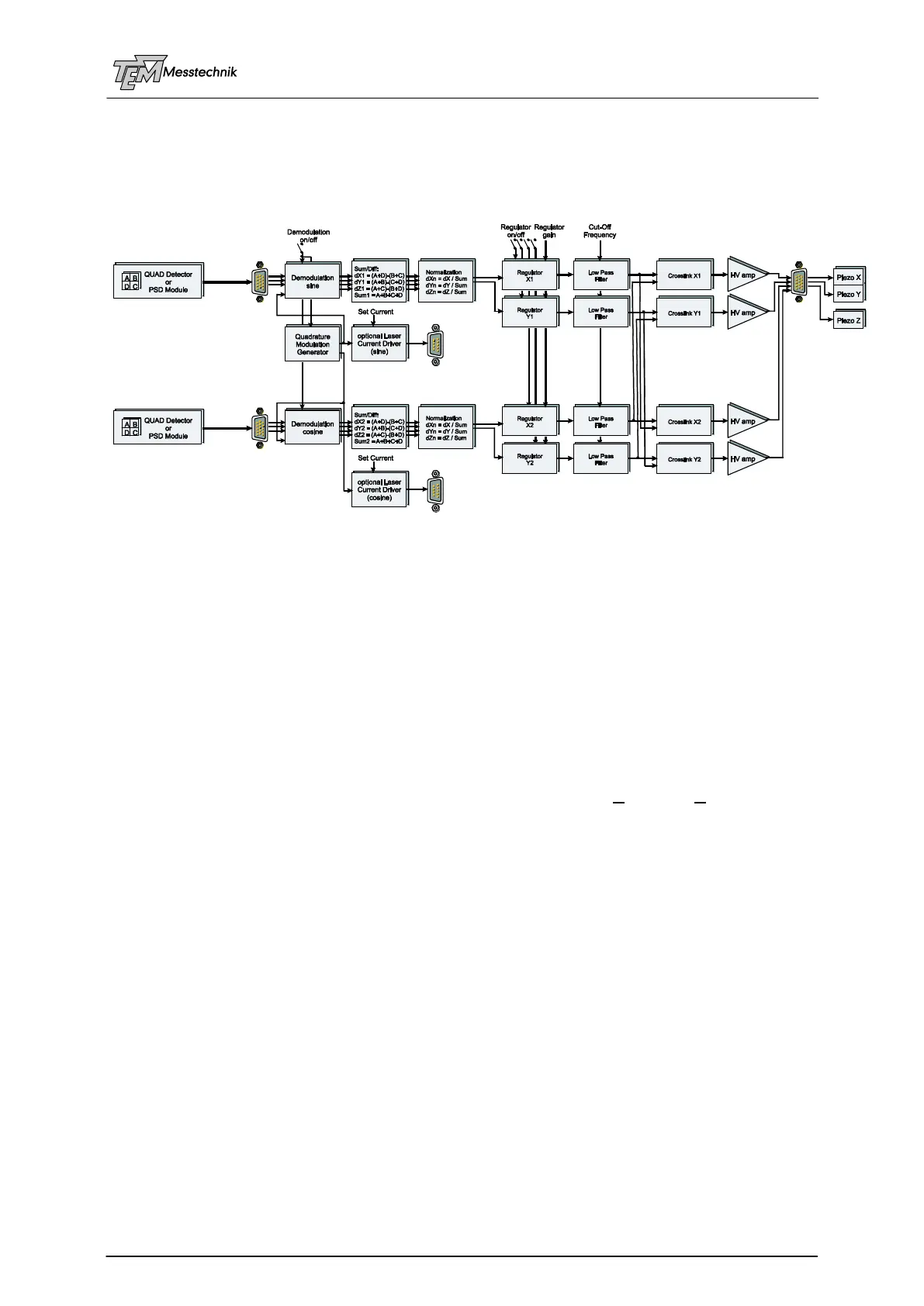
2 Block Diagram Aligna
®
4D
In the following, the block diagram of the Aligna
®
4D electronics is described.
Note: This chapter is preliminary: It still contains additional information related to former ver-
sions.
Two 2D sensors “PSD 2D” (or one 4D sensor “PSD 4D”) detect both 2D position (“X”, “Y”)
and 2D angle (“”, “”) of a laser beam. The detector electronics contain (dependent on the
detector type):
The position sensitive chip: A variety of detector sizes and types is available: 2x2 mm,
4x4 mm, 9x9 mm, 12x12 mm, others on request, as well as quadrant detectors of different
sizes. Different speed options are available, please refer to PSD manual.
The detectors are located at a small PCB, which also contains transimpedance amplifiers
and filter networks to achieve very linear low noise robust signals.
The detectors are connected with the cables “PSD 1” to “PSD 4” with the Aligna
®
4D electron-
ics, which contains following functions.
signal range and clip check for each channel Ax, Ay, Bx, By
Input Cross-link Matrix circuitry (ICL Matrix) (calculation of pure Angle and BeamPosition
signals)
Set point definition (SetpAx, SetpAy, SetpBx, SetBy), fixed, external analog control or digital
control (including test generator)
Error calculation (4D actual position – 4D set position)
Gain and regulator control logic
Four PIDT
2
regulators
Output Cross-link Matrix circuitry (OCL Matrix) (calculation of the combination movement)
Monitor multiplexer for observation of all relevant signals
HV Piezo amplifiers
Motor Drivers
MicroController Module, including USB Interface, Serial Interface, (Ethernet optionally)
Power Supply