LLZ 421
Repair Operation and Maintenance
ILS 420
6−58 Ed. 01.10SOAC
JP1
CLRSBOCLRCSBCRSSBO
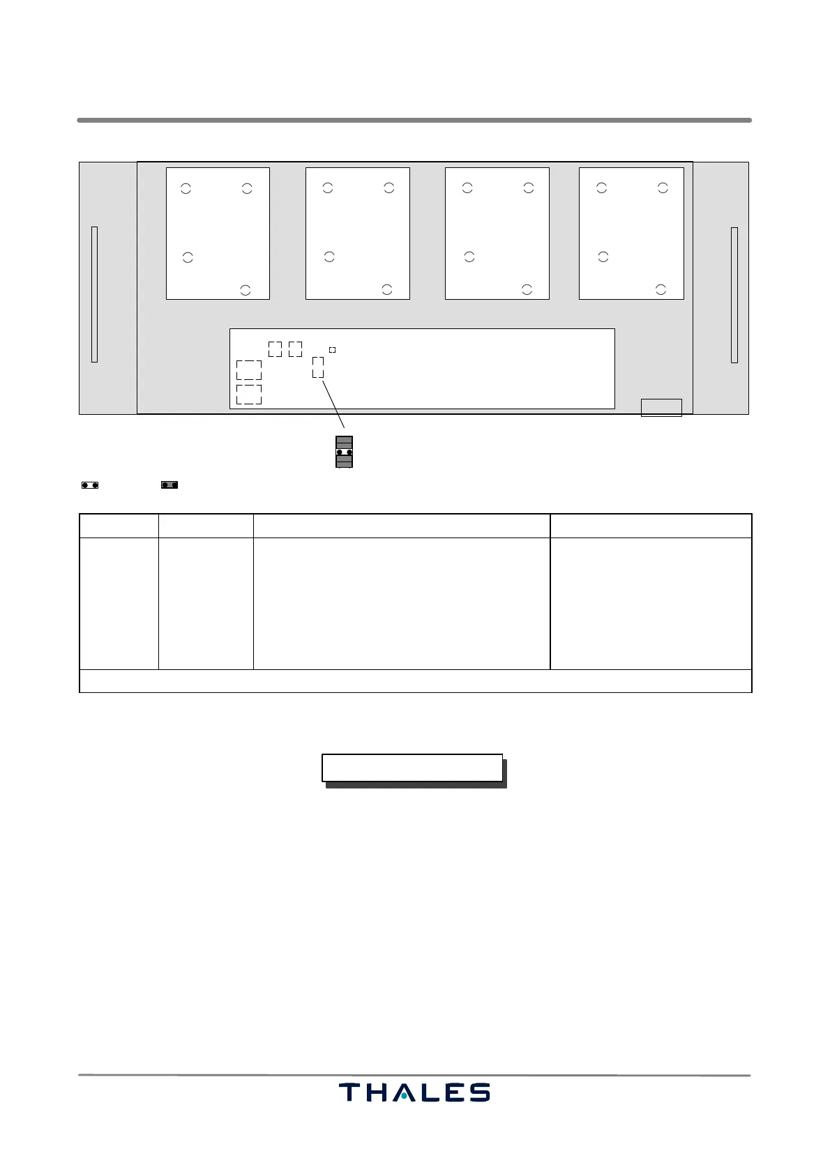
Driver and Bias supply
J31
J10J12
J11
J28
J7J9
J8
J27
J4J6
J5
J26
23 4
CRSCSB
J1J3
J2
J25
1
setopen
below cover, normally not accessible
10
8
6
4
2
9
7
5
3
1
TP1
JP1
view on component side
Jumper POSITION DEFINITION REMARKS
Jumper
bank JP1
9−10
7−8
5−6
3−4
1−2
set
set
open
set
set
Used for DC−DC test purposes:
disconnection of DC−DC supply
+5V In
+5V In
GND
−140V In
−140V In
Factory use only
default setting
default setting
default setting
default setting
default setting
7 PIN−Diode Transfer Switch 120622−002 (83138 28100) 1 of 1
WARNING
Do not remove the cover of the driver and bias supply and the PIN−Diode switches.
Switch off DC−supply before working on the subassembly with removed covers. Regard
that the internal generated PIN−Diode reverse bias supply is −140 V/30 mA, to be mea-
sured at TP1.