Function of each device
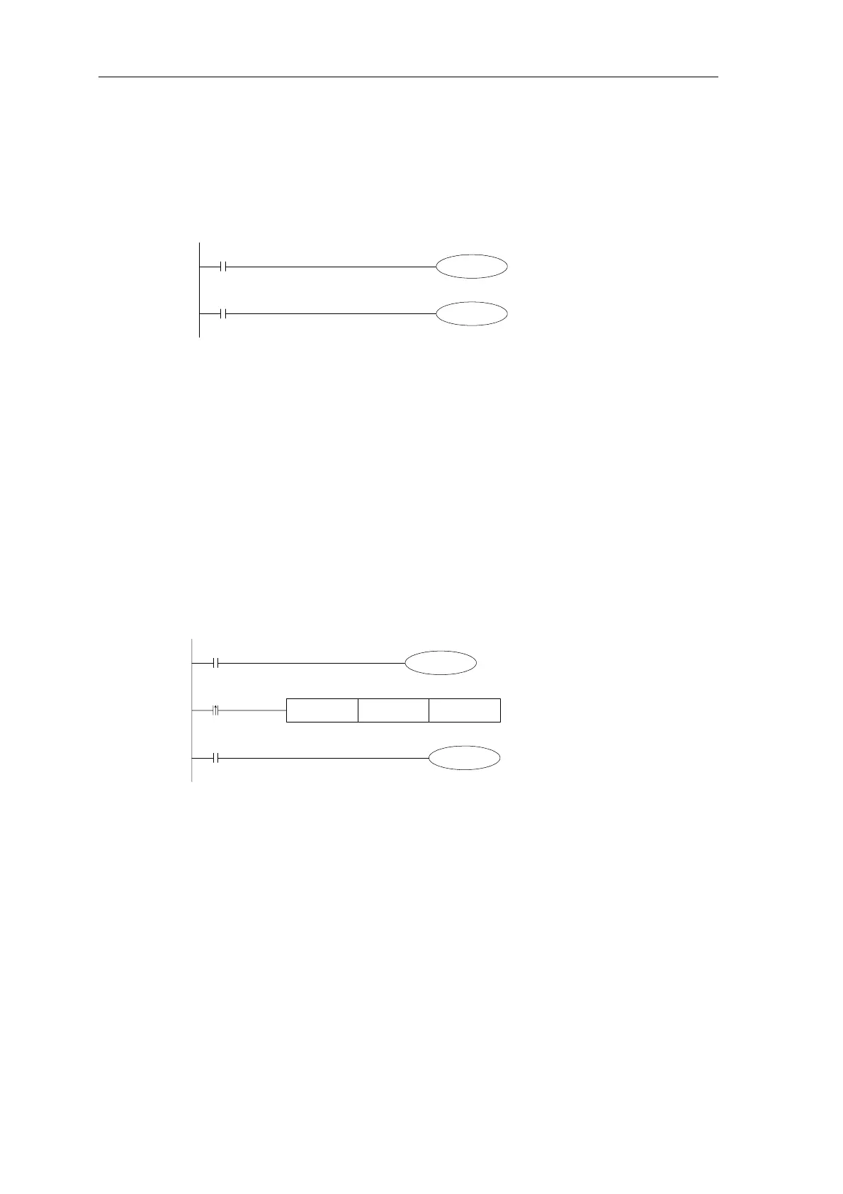
D0.4
Y0
D5[D1].4
Y1
MOV D0T11
M0
T11
Y1
X0
T11
K99
5、 Tag type:P,I
e.g.:P means the tag which using CJ instruction or CALL instruction which could jump; I
means interrupt tag.
3、 Bit of word device
Format:Dn.m
Register could carry on bit searching address, e.g. Dn.m means number “m” bit of Dn data
register(0≤m≤15)。
4、 T/C means the difference of register’s word and bit
To T and C register, Tn/Cn means be a bit register or a word register should be
distinguished by the instructions.
T、C could denote the status of timer、counter, or the current value of time、counter, it is
distinguished by the instructions.
In the preceding example, D0.4 means when the No.4 bit of D0 is 1, Y0 set ON;
D5[D1].4 means bit searching address with offset, if D1=5,it says D5[D1] means the number 4
bit of D10.
z The bit of word device with offset is denoted as Dn[Dm].x
z Please note, to the bit of word device, they couldn’t combined to be word device.
In the preceding example,MOV T11 D0,T11 means word register;
LD T11,T11 means bit register.
38