6 Controller Architecture
Trident Planning and Installation Guide
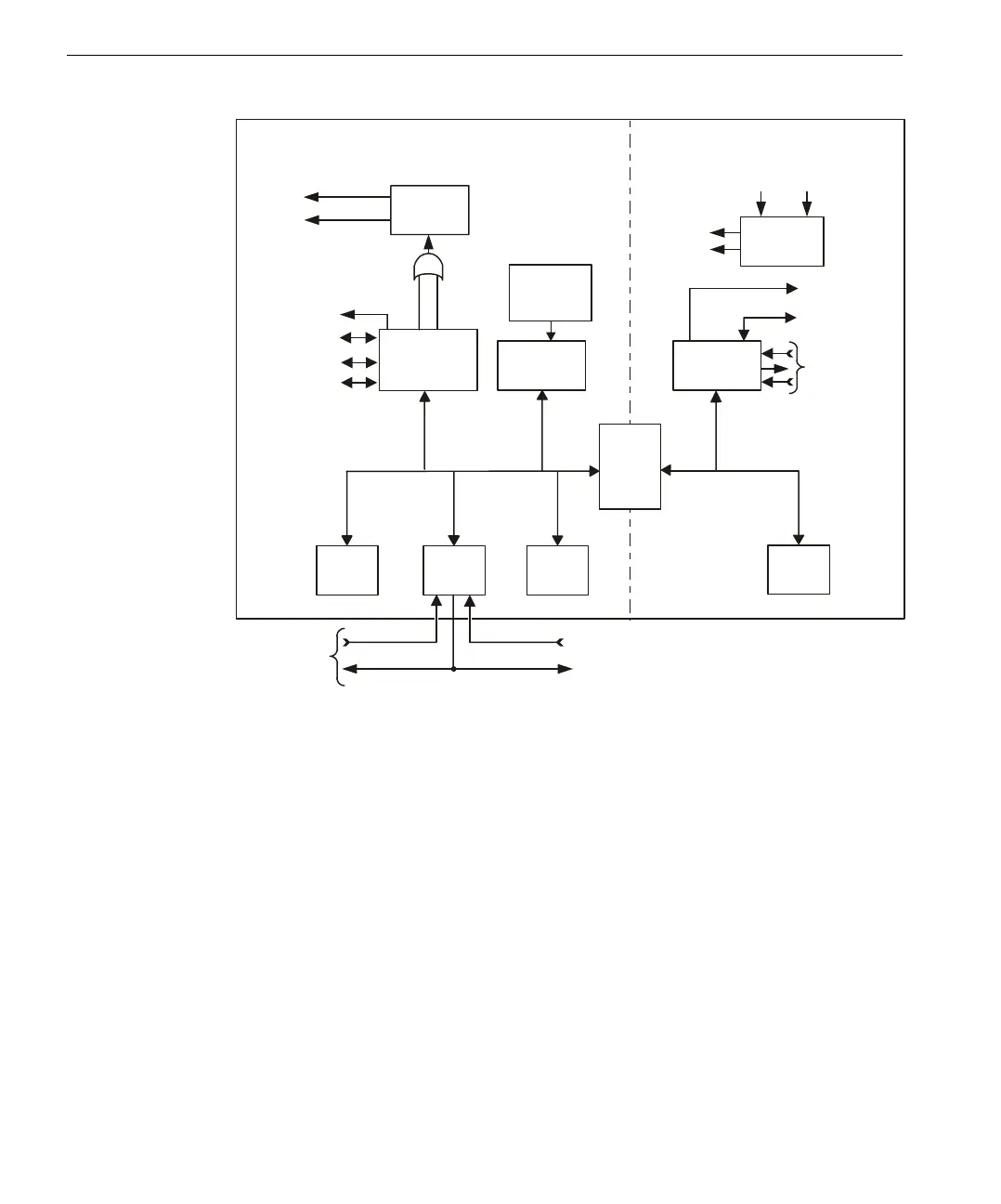
Using the table of output values, the I⁄O control processor generates smaller tables,
each corresponding to an individual output module. Each small table is transmitted
to the appropriate channel of the corresponding output module over the I⁄O bus. For
example, MP A transmits the appropriate table to channel A of each output module
over I⁄O bus A. The transmittal of output data has priority over the routine scanning
of all I⁄O modules.
Each MP provides a 16-megabyte DRAM for the user-written application,
sequence-of-events (SOE) and I⁄O data, diagnostics, and communication buffers.
(For more information about SOE, see the Sequence of Events Recorder User's
Manual.)
The application is stored in flash EPROM and loaded in DRAM for
execution. The MPs receive power from redundant 24 volts DC power sources. If
an external power failure occurs, all critical retentive data is stored in NVRAM. A
failure of one power source does not affect controller performance. If the controller
loses power, the application and all critical data are retained indefinitely.
Main Processor
Architecture
Modbus (DB-9)
Reserved (DB-9)
Redundant
Alarm
Relays
Debug (RJ-12)
Alarm 1
Alarm 2
Clock/NVRAM
8 KB
Program Processor
DRAM
16 MB
DRAM
16 MB
Flash
4/8 MB
Tr iBu s
FPGA
Tribus
(to other MPS)
Up Stream
Up Stream
Down Stream
Down Stream
Diagnostic Bus
Channels
(to other MPs)
I/O Bus
Debug (RJ-12)
MPC860A
I/O Processor
Program
Alarm
System
Alarm
Ethernet
Network (RJ-45)
3.6 V
Battery
and Monitor
36-Bit Bus
36-Bit Bus
Dual 24 V
Power Inputs
Dual-Power
Regulators
+5 V
+3.3 V
Shared
Memory
128 K
MPC860A