58
CHAPTER 6 - DETAILED PARAMETER DESCRIPTION
NOTE!
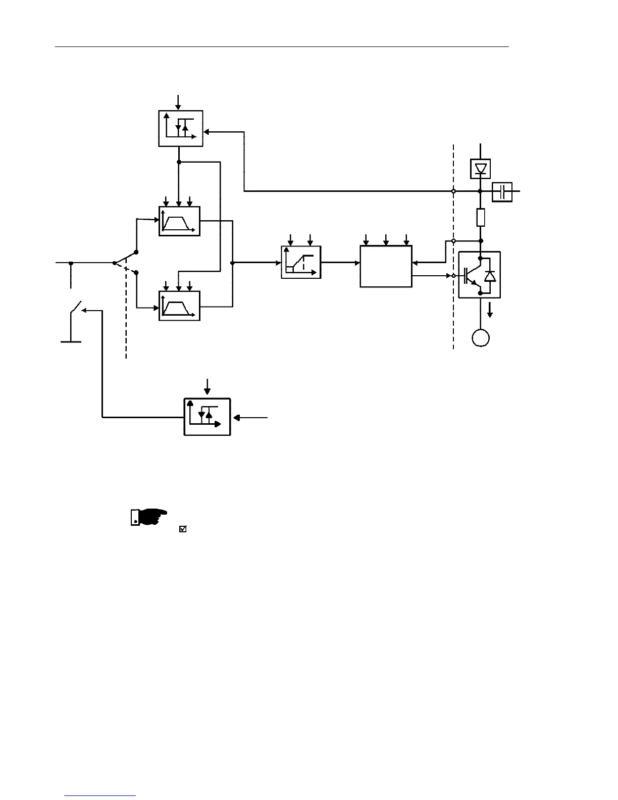
In V/F control mode (P202 = 0 or 1), Fe = F* (see Fig. 6.1) if P138 = 0
(slip compensation disabled). If P138 0, see figure 6.9 for the
relation between Fe and F*.
Figure 6.2 - Inverter block diagram
Fe
Command via
Digital Input
(DI)
Acceleration and
Deceleration
Ramp 2
Acceleration
and Deceleration
Ramp
P102
P103
P100
P101
DC Link
Regulation
P151
U
d
P133 P134
Frequency
Reference
Limits
P202
P295
Inverter
Control
(V/F or
Vector)
P136, P137,
P138, P142,
P145
PWM
P169
I
s
Output
Current
Limiting
I
U
d
Po wer
Supply
IM
3Ø
I
s
P169
V
s
P151