KCU116 Board User Guide 43
UG1239 (v1.2) September 28, 2018 www.xilinx.com
Chapter3: Board Component Descriptions
Note: The SFP0_TX_DISABLE/SFP1_TX_DISABLE I/O standard LVCMOS33 and the GTY TX/RX
connections I/O standard are not applicable.
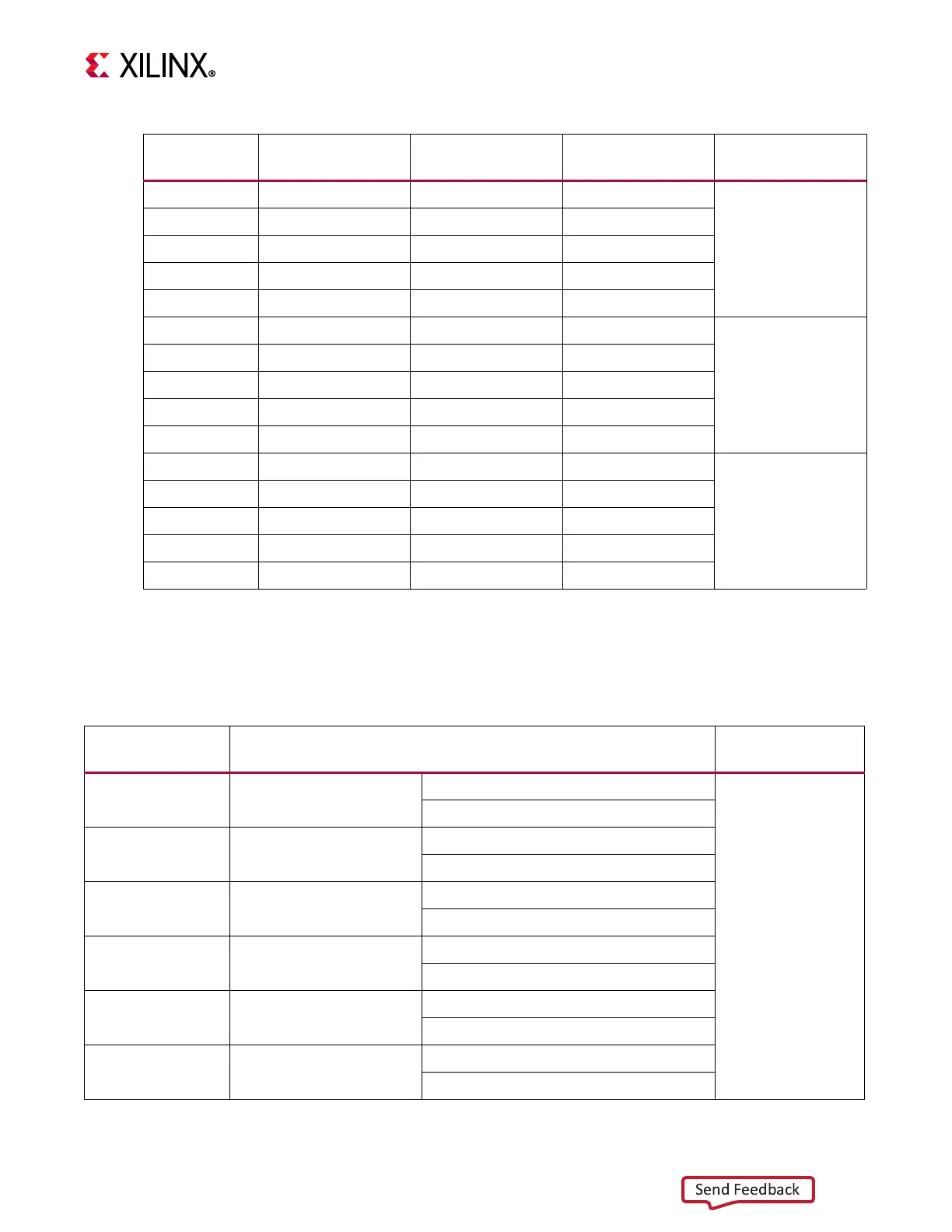
Table 3-11 lists the zSFP+ module control and status connections.
K2 SFP1_RX_P 13 RD_P
zSFP1 J3
K1 SFP1_RX_N 12 RD_N
L5 SFP1_TX_P 18 TD_P
L4 SFP1_TX_N 19 TD_N
AA14 SFP1_TX_DISABLE_B 3 TX_DISABLE
H2 SFP2_RX_P 13 RD_P
zSFP2 J4
H1 SFP2_RX_N 12 RD_N
J5 SFP2_TX_P 18 TD_P
J4 SFP2_TX_N 19 TD_N
AA15 SFP2_TX_DISABLE_B 3 TX_DISABLE
F2 SFP3_RX_P 13 RD_P
zSFP3 J6
F1 SFP3_RX_N 12 RD_N
G5 SFP3_TX_P 18 TD_P
G4 SFP3_TX_N 19 TD_N
Y15 SFP3_TX_DISABLE_B 3 TX_DISABLE
Table3‐10: KCU116 FPGA U1 to zSFP0‐zSFP3 Module Connections (Cont’d)
FPGA (U1) Pin
Schematic Net
Name
Pin Number Pin Name SFP/SFP+ Module
Table3‐11: zSFP0‐ zSFP3 Module Control and Status Connections
zSFP Control/
Status Signal
Board Connection SFP Module
SFP_TX_FAULT Test Point J57
High = Fault
zSFP0 J1
Low = Normal operation
SFP_TX_DISABLE Jumper J16
Off = SFP Disabled
On = SFP Enabled
SFP_MOD_DETECT Test Point J64
High = Module not present
Low = Module present
SFP_RS0 PU R25/ PD R30
PU R25 = Full RX bandwidth
PD R30 = Reduced RX bandwidth
SFP_RS1 PU R227/ PD R142
PU R227 = Full RX bandwidth
PD R142 = Reduced RX bandwidth
SFP_LOS Test Point J68
High = Loss of receiver signal
Low = Normal operation