ABCDEFGH I J KL
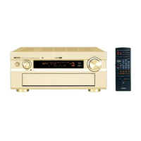
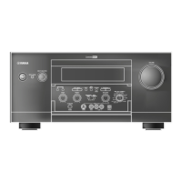
RX-V3300/DSP-AZ2
75
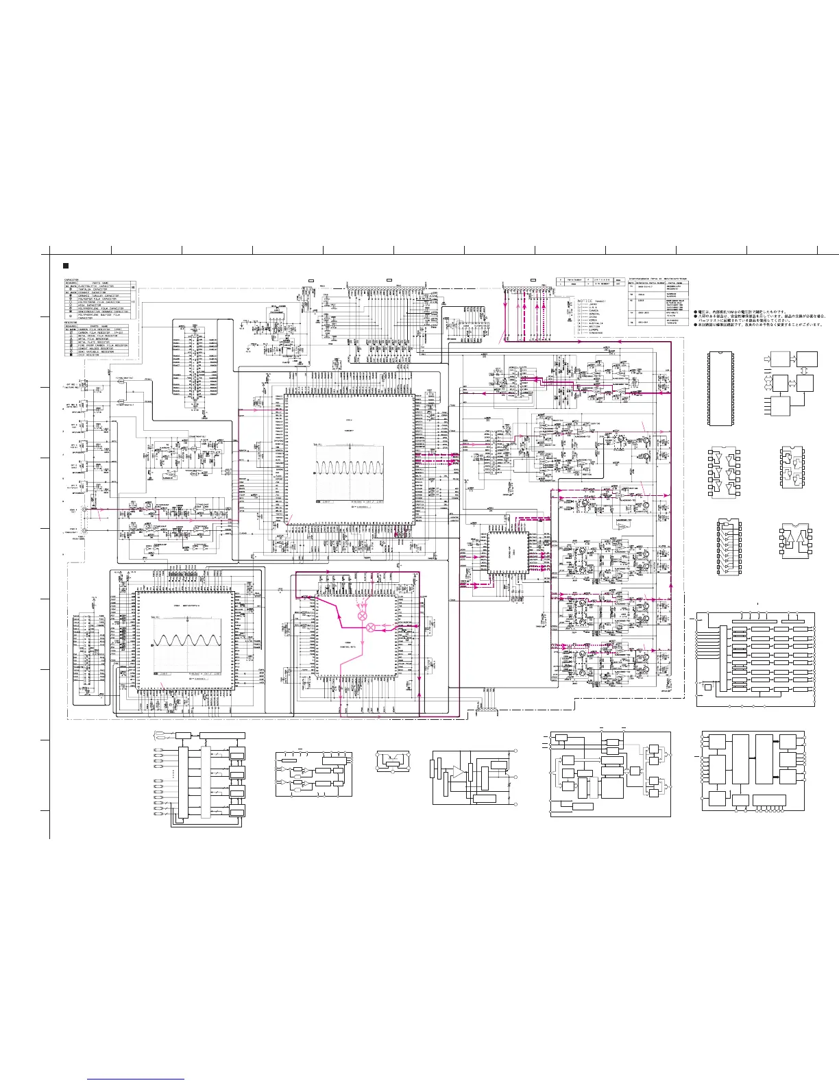
SCHEMATIC DIAGRAM (DSP)
1
2
3
4
5
6
7
8
9
Point 1 Pin 1 of IC514
Point 2 Pin 9 of IC504
LEVEL CONVERT & SIGNAL DETECT
DSP/DOLBY/DTS
4M DRAM
D/A CONVERTER
D/A CONVERTER
A/D CONVERTER
BUFFER
REGULATOR
DIGITAL OUT INHIBIT
DUTY CORRECTOR
PLD
DECODER
SRAM
Page 77
to OPERATION (3)
Page 76
to FUNCTION
2
1
6
5
4
3
13
12
9
10
11
8
E1Page 76
to FUNCTION
D1
H5
59
6
8
59
6
8
1113
10
12
3
1
4
2
3
1
1
11
8
7
14
4
2
7
3
2
12
13
9
10
7
14
5
6
8
4
11
13
14
10
7
12
1
8
2
3
1
8
2
3
7
4
5
6
2
3
5
6
2
3
6
5
5
3
2
6
5
6
1
4
7
1
7
7
8
4
8
1
7
3
2
4
1
2
3
8
1
5
6
4
7
8
4
8
2
3
5
6
7
5
6
2
3
7
1
1
8
4
4
8
7
4
5
6
★ All voltages are measured with a 10MΩ/V DC electric volt meter.
★ Components having special characteristics are marked s and must be
replaced with parts having specifications equal to those originally
installed.
★ Schematic diagram is subject to change without notice.
x: NOT USED
O:USED / APPLICABLE
IC500: IS61LV6416-15K
64k x 16 High-speed CMOS Static RAM
1
2
3
4
5
6
7
8
9
10
11
12
13
14
15
16
17
18
19
20
21
22
A15
A14
A13
A12
A11
/CE
I/O0
I/O1
I/O2
I/O3
Vcc
GND
I/O4
I/O5
I/O6
I/O7
/WE
A10
A9
A8
A7
NC
A0
A1
A2
/OE
/UB
/LB
I/O15
I/O14
I/O13
I/O12
GND
Vcc
I/O11
I/O10
I/O9
I/O8
NC
A3
A4
A5
A6
NC
44
43
42
41
40
39
38
37
36
35
34
33
32
31
30
29
28
27
26
25
24
23
A0 - A15
VCC
GND
/CE
/OE
/WE
/UB
/LB
I/O0 - I/O7
Lower Byte
I/O8 - I/O15
Upper Byte
DECODER
I/O
DATA
CIRCUIT
CONTROL
CIRCUIT
COLUMN I/O
64k X 16
MEMORY ARRAY
IC501~502: TC74HCU04AF
Hex Inverters
1A
1Y
2Y
VCC
6A
1
2
3
4
11
2A 6Y
5A
12
13
14
3A
3Y
5Y
4A
5
6
7
4Y8
9
10
GND
4B13
4A12
4Y11
3B10
3A9
3Y8
1B 2
1Y 3
2A 4
2B 5
2Y 6
GND 7
IC503: TC74HCT00AF
Quad 2-Input Nand Gate
Vcc141A 1
IC505: TC74VHCT541AF
3-State Buffer
Vcc20
/G219
Y118
Y217
Y316
Y415
Y514
/G1 1
A1 2
A2 3
A3 4
A4 5
A5 6
A6 7
Y613
Y712
Y811
A7 8
A8 9
GND 10
IC507~509, 518~523: NJM2068MD
IC513: NJM2904M
Dual OP-Amp.
–+
OUT
1
–IN
1
–V
CC
+V
CC
OUT
2
1
2
3
4
5
+IN
1
–IN
2
+IN
2
–+
6
7
8
IC510 : CS4382-KQR
8-Channel D/A Converter
+2
Volume Control ∆∑ DAC Analog Filter
Mixer
Interpolation Filter
Serial Port
Control Port (Stand-Alone Mode Select)
42
19
43
7
10
11
14
4 5 31 32
15 16 17 18
39
40
AOUTA1+
AOUTA1-
Volume Control ∆∑ DAC Analog FilterInterpolation Filter
38
37
AOUTB1+
AOUTB1-
Volume Control ∆∑ DAC Analog Filter
Mixer
Interpolation Filter
35
36
AOUTA2+
AOUTA2-
Volume Control ∆∑ DAC Analog FilterInterpolation Filter
34
33
AOUTB2+
AOUTB2-
Volume Control ∆∑ DAC Analog Filter
Mixer
Interpolation Filter
29
30
AOUTA3+
AOUTA3-
Volume Control ∆∑ DAC Analog FilterInterpolation Filter
28
27
AOUTB3+
AOUTB3-
Volume Control ∆∑ DAC Analog Filter
Mixer
Interpolation Filter
25
26
AOUTA4+
AOUTA4-
Volume Control ∆∑ DAC Analog FilterInterpolation Filter
24
23
AOUTB4+
AOUTB4-
21
VQ
20
FILT+
VD
GND
GND
VA
RST
VLS
LRCK1
LRCK2
SDIN2
SDIN4
9
12
8
13
SCLK1
SCLK2
SDIN1
SDIN3
DSDxx
6
8
MCLK
DSD_SCLK(M3)
SCL/CCLK (M2)
SDA/CDIN(M1)
AD0/CS (M0)
VLC
External Mute Control
41 22
MUTEC1
MUTEC234
Input
Interface
Digital
Filter
LRCK
DATA
BCK
RST
MUTE
FMT0
2
ZEROL
3
ZEROR
Function
Control
Interface
IOUTL+
4
5
6
System
Clock
Manager
System
Clock
ZERO
Detect
9
VDD
8
DGND
23
VCC1
24
VCC2
28
VCC3
18
AGND1
27
AGND2
Power
Supply
SCKI
7
15
12
1
FMT1
FMT2
Current
Segment
DAC
Current
Segment
DAC
Bias
&
Vref
Advanced
Segment
DAC
Modulator
DEMP0
14
10
DEMP1
11
13
25
IOUTL-
26
IOUTR-
16
IOUTR+
17
VCOM2
20
IREF
21
VCOM1
19
VCOM3
22
IC511: PCM1730E-1/2K
D/A Converter
IC515: MSM514260E-60JS
4Mbit DRAM
Timing
Generator
I/O
Controller
Output
Buffers
Input
Buffers
Input
Buffers
Output
Buffers
I/O
Controller
Column Decoders
RAS
Refresh
Control Clock
14
WE
13
9
9
LCAS
29
UCAS
A0~A8
28
VCC
20
VSS
21
Sense Amplifiers
I/O
Selector
Memory
Cells
OE
27
DQ9~DQ16
Column
Address
Buffers
Internal
Address
Counter
Row
Address
Buffers
On Chip
VBB Generator
Row
Deco-
ders
Word
Drivers
9
9
16 16
8
8
8
8
8
8
DQ1~DQ8
8
8
IC516: µPC29M33T-E1
Voltage Regulator
3
OUTPUT
1
INPUT
2
GND
Safety Drive
Limiter
Excessive Electric
Current Protection
Sudden Current
Protection
Starter Circuit
Driver
Standard Voltage
Overheat Protection
Amp.
IC517: PQ070XZ5MZP
Regulator
1
Vin
Vc
3
Vo
42
Vadj
5
GND
15
CMOUT
16
AINL-
17
AINL+
9
SDATA
19
DIF1
20
DIF0
Voltage Reference
Digital Decimation
Filter
LP Filter
S/H
S/H
Comparator
Serial Output Interface
+
–
+
–
+
–
High Pass
Filter
4
AGND
3
VA+
6
VD+
18
RSY
7
MCLK
2
OVFL
10
FRAME
8
SCLK
12
LRCK
5
DGND
11
PU
1
HP DEFEAT
IC524: CS5360-KSR
Stereo A/D Converter
DAC
14
AINR-
13
AINR+
Digital Decimation
Filter
LP Filter
Comparator
+
–
+
–
+
–
High Pass
Filter
DAC
IC526: XC9572XL-10TQ100C
CPLD
I/O
Function
Block 1
Macrocells
1 to 18
I/O
Blocks
JTAG
Controller
In-System Programming Controller
Fast CONNECT II Switch Matrix
I/O
I/O
I/O
I/O
I/O
I/O
I/O
I/O/GCK
I/O/GSR
I/O/GTS
2
54
18
1
JTAG Port
1
3
3
Function
Block 1
Macrocells
1 to 18
54
18
Function
Block 1
Macrocells
1 to 18
54
18
Function
Block 1
Macrocells
1 to 18
54
18
2.5
0
0
3.3
1.7
1.7
0.6
1.7
0.7
0
2.5
2.5
2.5
2.5
2.5
0
4.9
2.5
2.5
2.5
2.5
3.3
3.3
2.5
2.4
0
0
0
0
0
3.3
3.3
4.7
2.5
0
2.5
DIGITAL IN
1
FRONT L
REAR L
CENTER
MAIN L
MAIN L (ANALOG IN)
4.7
0
0
4.7
0
0
0
3.8
4.7
0
3.8
4.7
0
3.8
4.7
0
3.8
4.7
0
0
3.3
4.7
0.5
0.5
0.5
0.5
4.7
1.4
1.4
1.4
1.8
1.4
3.1
1.0
1.7
0
0
0
0
0
0
0
0
0
2.5
3.5
0
0
0
4.7
0
4.7
4.7
4.7
0
0
0
0
4.7
4.7
2.5
0.1
0.1
3.5
0
0
0
0
0
4.7
4.7
0
0
0
0
0
3.4
0
0
3.4
0
0
0
0
0
0
0
0
0
3.4
0
0
0
0
0
0
0
3.4
0
0
0
0
0
0
3.4
0
0
0
0
0
0
0
0
4.7
4.7
0
0
4.7
3.0
2.5
0.4
3.0
~
4.7
~
0
0.5
0.5
0.5
0.5
0
0.5
0.5
0.5
2.0
0
0.5
2.2
~
2.3
2.2
~
~
~
4.7
3.4
4.7
3.6
2.6
0
3.8
3.8
0.1
2.7
0.1
4.8
0
3.8
0
4.7
0.1
0
0.3
4.7
1.7
3.3
3.3
0
0
0
0
2.6
0
0
0
~
~
0.4
0
~
~
1.7
~
1.0
~
2.3
3.3
0
1.8
2.0
3.1
2.3
0.5
0.5
0.5
0.5
0.5
0.5
0.5
3.3
0
1.4
1.4
1.4
1.4
0
0
3.4
0
0.5
0.5
0
1.6
1.6
0.2
3.3
0
0
3.3
0.2
0
0
0
1.1
3.3
2.3
2.1
0
4.7
3.3
0.2
0
1.3
1.7
1.7
0
1.3
2.0
1.3
0
0
0
0
0
0.5
0.5
0.5
2.6
0
3.3
3.3
0
3.3
3.3
3.3
3.3
3.3
0.1
0.1
0.1
0.1
1.7
1.7
1.7
1.7
1.7
1.7
1.7
0
1.7
1.7
1.7
2.6
0
0
0
3.3
0.7
0.6
0
0
0
4.8
4.8
3.3
0
3.3
0
2.7
02.70.3 4.6 4.8
2.7 4.8
0
2.50
0
4.9
2.5
3.44.9
0
00
2.51.8
2.51.8
1.8
3.0
4.9
2.5
4.9
0
2.5
0
2.5
2.5
4.9
2.5
0
4.9
2.5
2.5
4.9
0
2.5
2.5
2.5
2.5
11.4
2.5
2.5
2.5
11.8
2.5
2.5
2.5
-11.8
2.5
-11.2
0
0
0
0
1.4
1.4
1.4
11.4
-11.8
1.4
2.5
0
0
0
0
2.5
2.5
2.5
2.5
11.4
-11.8
2.4
2.4
2.5
3.3 4.9
0
2.5
2.5
4.9
2.5
2.5
4.9
2.7
2.5
2.5
2.4
0
1.7
1.3
1.7
1.7
0
0
3.3
3.3
0
3.3
0
2.5
2.5
2.5
-11.8
11.4
2.4
2.4
0
-11.2
0
0
-11.2
0
0
0
0
0
0
11.4
-11.8
0
0
0
0
0
-11.2
-11.2
0
0
0.6
1.8
0
00
0
3.4
0
1.8
1.9
1.9
0
0
0
0
0
0
-11.2
-11.8
2.8
-11.3
11.4
2.9
2.9
0
0
-11.2
0
0
1.8
0
0
0
0
0
0
0
-11.2
-11.8
-11.3
11.4
0
0
-11.2
1.9
0.1
0.1
0.1
0.1
0
0
0
0
0
0
1.9
1.9
1.9
0
0
0
0
0
0
-11.2
-11.8
-11.3
0
0
0
0
0
0
0
0
0
0
-11.3
-11.3
11.4
0
0
2.5
-11.8
0
1.7
0
1.6
0
0
0
0
0
~
4.8
4.8
0
4.6
4.6
0
1.3
3.3
0
3.3
0
1.7
1.7
0
1.7
1.7
2.0
0
1.3
2.6
2.6
0
1.7
0
0
0
0
0
0
3.4
1.7
0
0
1.7
3.3
0
1.7
0
0
1.7
0
1.7
0
1.7
3.3
1.7
0
2.9
0
0
3.3
3.3
0
3.3
0
1.3
0
2.0
3.3
1.3
0
0
0
0
0
3.3
0
2.9
0
0
3.1
3.2
0
0
0.3
0
0
2.0
3.3
2.6
0
3.1
3.1
0
~
2.9
3.1
3.4
3.4
3.4
0
2.6
0
0
0
0
0
0
0
3.4
3.4
0
2.0
0
1.7
1.7
0
3.3
0
0
0
0
0
0
0
3.3
4.7
0
2
0
0
0
0
0
0
0
0
0
3.4
0
0
0
0
0
2.6
0
0
0
0
0
0
0
4.8
0
0
0
0
0
4.6
0.1
0
0.3
0
3.1
4.8
0
~
0
0
0
47/50
47/50
47/50
47/50
47/50
4.3K
4.3K
4.3K
2.7K
2.7K
2.7K
18K18K
2.7K
4.3K