EasyManuals Logo

Abov MC96F6332D User Manual

Default Icon
327 pages
To Next Page IconTo Next Page
To Previous Page IconTo Previous Page
Page #244 background imageLoading...
Page #244 background image
MC96F6432
244 June 22, 2018 Ver. 2.9
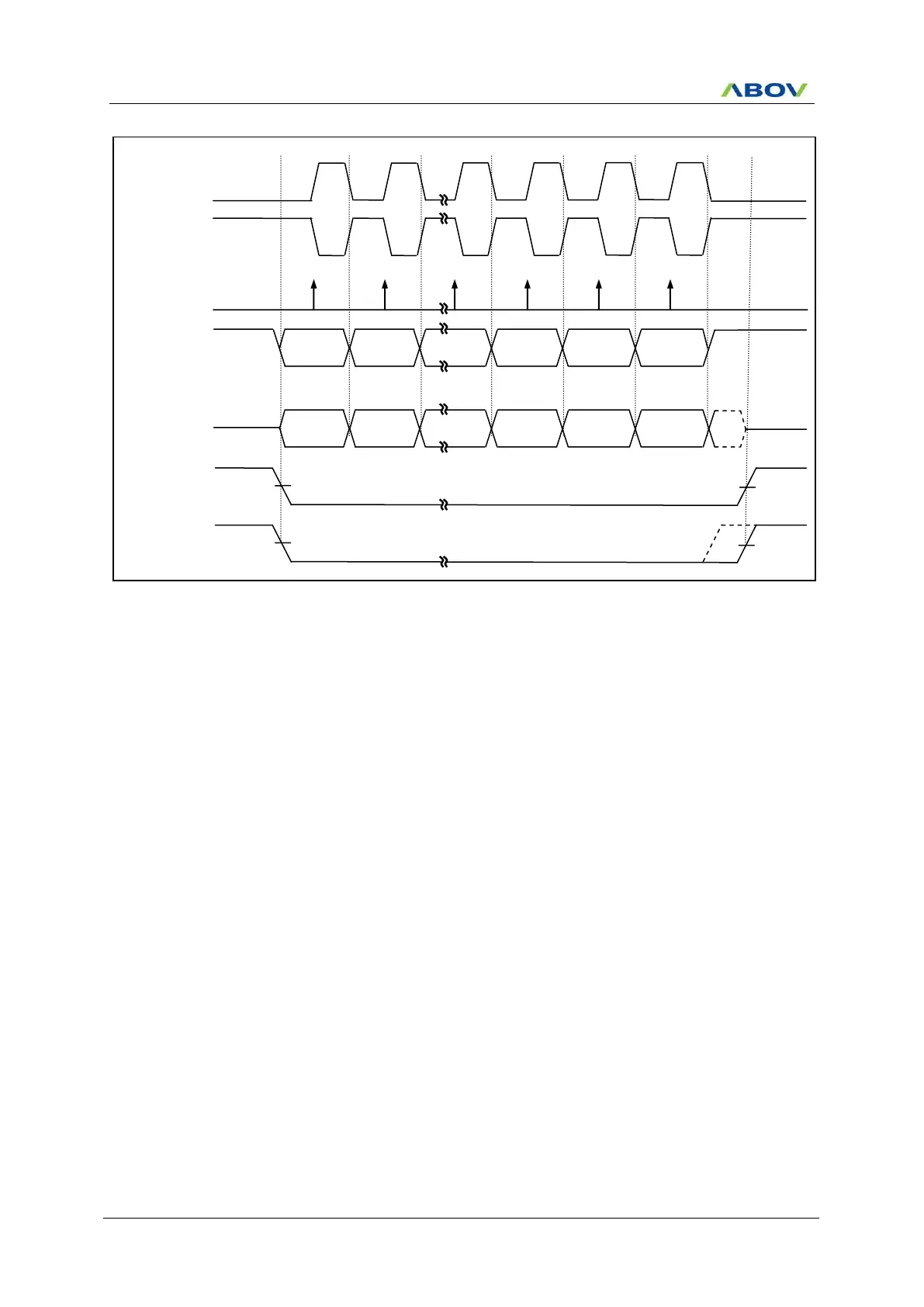
Figure 11.85 USI1 SPI Clock Formats when CPHA1=0
When CPHA1=0, the slave begins to drive its MISO1 output with the first data bit value when SS1 goes to active
low. The first SCK1 edge causes both the master and the slave to sample the data bit value on their MISO1 and
MOSI1 inputs, respectively. At the second SCK1 edge, the USI1 shifts the second data bit value out to the
MOSI1 and MISO1 outputs of the master and slave, respectively. Unlike the case of CPHA1=1, when CPHA1=0,
the slave’s SS1 input must go to its inactive high level between transfers. This is because the slave can prepare
the first data bit when it detects falling edge of SS1 input.
SCK1
(CPOL1=1)
MISO1
MOSI1
SCK1
(CPOL1=0)
/SS0 OUT
(MASTER)
BIT7
BIT0
/SS1 IN
(SLAVE)
BIT6
BIT1
…
…
BIT2
BIT5
BIT0
BIT7
BIT1
BIT6
SAMPLE
MSB First
LSB First

Table of Contents

Questions and Answers:

Question and Answer IconNeed help?

Do you have a question about the Abov MC96F6332D and is the answer not in the manual?

Abov MC96F6332D Specifications

General IconGeneral
BrandAbov
ModelMC96F6332D
CategoryMicrocontrollers
LanguageEnglish

Related product manuals