MC96F6432
288 June 22, 2018 Ver. 2.9
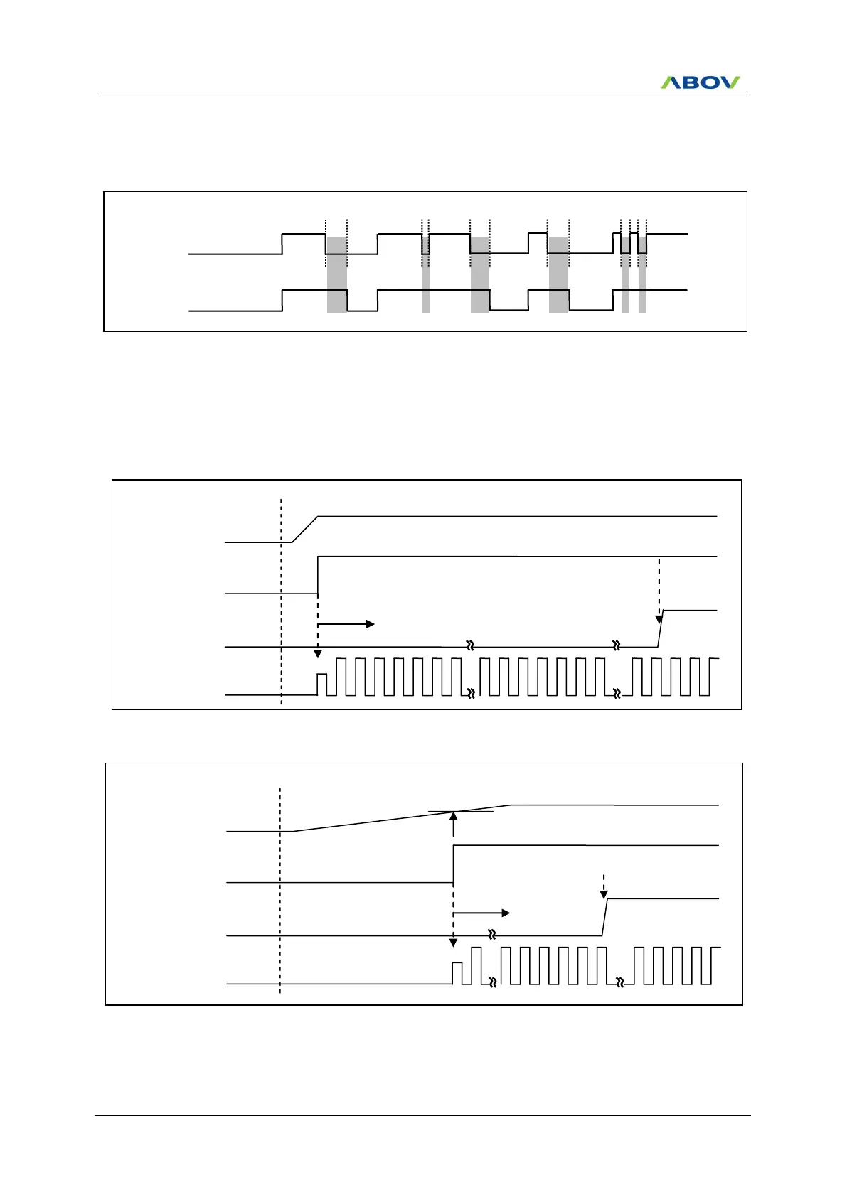
13.4 RESET Noise Canceller
The Figure 13.2 is the noise canceller diagram for noise cancellation of RESET. It has the noise cancellation
value of about 2us (@V
DD
=5V) to the low input of system reset.
Figure 13.2 Reset noise canceller timer diagram
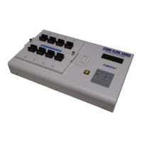
13.5 Power on RESET
When rising device power, the POR (Power On Reset) has a function to reset the device. If POR is used, it
executes the device RESET function instead of the RESET IC or the RESET circuits.
Figure 13.3 Fast VDD Rising Time
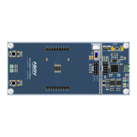
Figure 13.4 Internal RESET Release Timing On Power-Up
Slow VDD Rise Time, min. 0.05V/ms
Fast VDD Rise Time, max 30.0V/ms