MC96F6432
June 22, 2018 Ver. 2.9 297
14. On-chip Debug System
14.1 Overview
14.1.1 Description
On-chip debug system (OCD) of MC96F6432 can be used for programming the non-volatile memories and on-
chip debugging. Detail descriptions for programming via the OCD interface can be found in the following chapter.
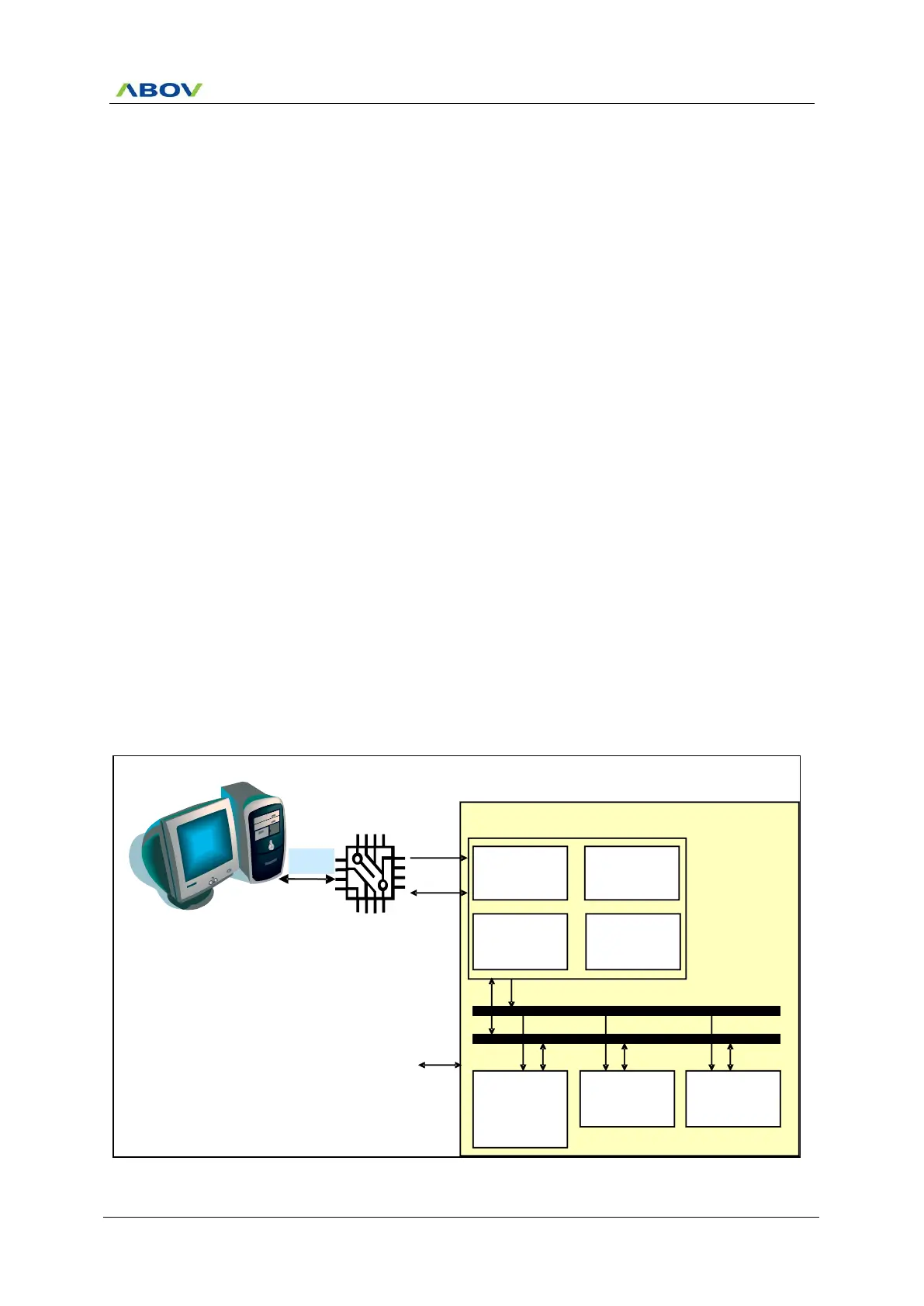
Figure 14.1 shows a block diagram of the OCD interface and the On-chip Debug system.
14.1.2 Feature
• Two-wire external interface: 1-wire serial clock input, 1-wire bi-directional serial data bus
• Debugger Access to:
− All Internal Peripheral Units
− Internal data RAM
− Program Counter
− Flash and Data EEPROM Memories
• Extensive On-chip Debug Support for Break Conditions, Including
− Break Instruction
− Single Step Break
− Program Memory Break Points on Single Address
− Programming of Flash, EEPROM, Fuses, and Lock Bits through the two-wire Interface
− On-chip Debugging Supported by Dr.Choice
®
• Operating frequency
Supports the maximum frequency of the target MCU
Figure 14.1 Block Diagram of On-Chip Debug System
Target MCU internal circuit