EasyManua.ls Logo

Abov MC96F6332D User Manual

Default Icon
327 pages
To Next Page IconTo Next Page
To Previous Page IconTo Previous Page
Page #76 background imageLoading...
Page #76 background image
MC96F6432
76 June 22, 2018 Ver. 2.9
9.4 P1 Port
9.4.1 P1 Port Description
P1 is 8-bit I/O port. P1 control registers consist of P1 data register (P1), P1 direction register (P1IO), debounce
enable register (P15DB), P1 pull-up resistor selection register (P1PU), and P1 open-drain selection register
(P1OD) . Refer to the port function selection registers for the P1 function selection.
9.4.2 Register description for P1
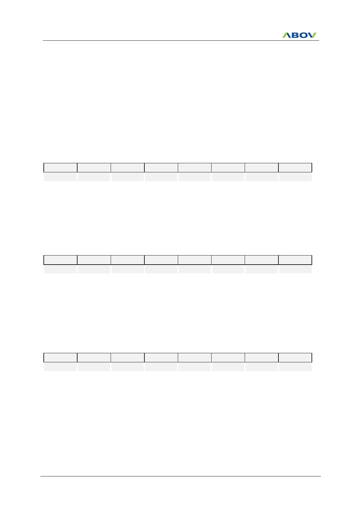
P1 (P1 Data Register) : 88H
7
6
5
4
3
2
1
0
P17
P16
P15
P14
P13
P12
P11
P10
R/W
R/W
R/W
R/W
R/W
R/W
R/W
R/W
Initial value : 00H
P1[7:0]
I/O Data
Note) Do not use the direct bit test and branch instruction for input port, more detail information is at
Appendix B.
Example) Avoid direct input port bit test and branch condition as below
If(P10) if(P1 & 0x01)
P1IO (P1 Direction Register) : B1H
7
6
5
4
3
2
1
0
P17IO
P16IO
P15IO
P14IO
P13IO
P12IO
P11IO
P10IO
R/W
R/W
R/W
R/W
R/W
R/W
R/W
R/W
Initial value : 00H
P1IO[7:0]
P1 Data I/O Direction
0
Input
1
Output
NOTE: EINT6/ENINT7/EINT11/EINT12/SS2/EC1 function possible
when input
P1PU (P1 Pull-up Resistor Selection Register) : ADH
7
6
5
4
3
2
1
0
P17PU
P16PU
P15PU
P14PU
P13PU
P12PU
P11PU
P10PU
R/W
R/W
R/W
R/W
R/W
R/W
R/W
R/W
Initial value : 00H
P1PU[7:0]
Configure Pull-up Resistor of P1 Port
0
Disable
1
Enable

Table of Contents

Question and Answer IconNeed help?

Do you have a question about the Abov MC96F6332D and is the answer not in the manual?

Abov MC96F6332D Specifications

General IconGeneral
Flash Memory32 KB
PWM Channels6
ADC Resolution10-bit
UART1
SPI1
I2C1
GPIO Pins36
CPU Speed16 MHz
Operating Temperature-40°C to 85°C
Core8-bit CISC core
PackageLQFP-48

Summary

Overview

Block Diagram

Pin Assignment

Package Diagram

Pin Description

Normal Pin Description

Details the function and shared pins for each device pin.

Normal Pin Description (Continued)

Provides final notes on pin description.

Port Structures

Electrical Characteristics

Absolute Maximum Ratings

Lists electrical parameters that should not be exceeded.

Recommended Operating Conditions

Specifies the voltage and temperature ranges for proper operation.

DC Characteristics

Lists DC electrical parameters.

DC Characteristics (Continued)

Continues the DC electrical parameters.

AC Characteristics

Lists AC electrical parameters and timing diagrams.

Recommended Circuit and Layout

Provides recommended circuit diagrams and layout guidelines.

Recommended Circuit and Layout with SMPS Power

Offers guidance for circuits using SMPS power.

Memory

Program Memory

Shows the map of the program memory.

Data Memory

Describes the internal data memory space.

SFR Map Summary

Provides a summary of the Special Function Register map.

SFR Map Summary (Continued)

Continues the SFR map summary.

SFR Map (Continued)

Continues the SFR map.

I/O Ports

I/O Ports

Provides a general overview of the I/O ports.

Interrupt Controller

Interrupt Vector Table

Lists all interrupt sources and their vector addresses.

IP (Interrupt Priority Register)

Describes the IP register for interrupt priority.

IP1 (Interrupt Priority Register 1)

Describes the IP1 register for interrupt priority.

Peripheral Hardware

Clock Generator

Provides an overview of the clock generator.

Clock Generator Register Description

Describes clock generator registers.

Basic Interval Timer

Provides an overview of the basic interval timer.

Watch Dog Timer

Provides an overview of the watchdog timer.

Register Description for Watch Dog Timer

Details WDTCNT, WDTDR, and WDTCR registers.

Watch Timer

Provides an overview of the watch timer's functionality.

Watch Timer Register Description

Describes WTCNT, WTDR, and WTCR registers.

Timer 0

Provides an overview of Timer 0.

8-Bit Timer/Counter Mode

Describes the 8-bit timer/counter mode for Timer 0.

8-Bit PWM Mode

Describes the 8-bit PWM mode for Timer 0.

8-Bit Capture Mode

Describes the 8-bit capture mode for Timer 0.

8-Bit Timer 0 Block Diagram

Shows the block diagram for Timer 0.

Timer 1

Provides an overview of the 16-bit Timer 1 module.

16-Bit Timer/Counter Mode for Timer 1

Shows the block diagram for 16-bit timer/counter mode.

Timer 2

Provides an overview of the 16-bit Timer 2 module.

16-Bit Timer/Counter Mode

Describes the 16-bit timer/counter mode for Timer 2.

16-Bit Capture Mode

Describes the 16-bit capture mode for Timer 2.

16-Bit PPG Mode

Describes the 16-bit PPG mode for Timer 2.

Timer 3, 4

Provides an overview of the Timer 3 and Timer 4 modules.

8-Bit Timer/Counter 3, 4 Mode

Describes the 8-bit modes for Timers 3 and 4.

16-Bit Timer/Counter 3 Mode

Describes the 16-bit mode for Timer 3.

8-Bit Timer 3, 4 Capture Mode

Describes the 8-bit capture mode for Timers 3 and 4.

8-Bit Capture Mode for Timer 3, 4

Shows the block diagram for 8-bit capture mode.

16-Bit Timer 3 Capture Mode

Describes the 16-bit capture mode for Timer 3.

10-Bit Timer 4 PWM Mode

Describes the 10-bit PWM mode for Timer 4.

Two 8-Bit Timer 3, 4 Block Diagram

Shows block diagram for 8-bit Timer 3/4.

Timer/Counter 4 Register Description

Describes Timer 4 registers.

T4CR (Timer 4 Control Register)

Details the T4CR register.

Buzzer Driver

Provides an overview of the buzzer driver.

Buzzer Driver Register Description

Describes BUZDR and BUZCR registers.

SPI 2

Provides an overview of the SPI 2 interface.

SPI 2 Register Description

Describes SPI 2 registers.

SPICR (SPI 2 Control Register)

Details the SPICR register.

12-Bit A/D Converter

Provides an overview of the 12-bit A/D converter.

Register Description for ADC

Describes ADCDRH, ADCDRL, ADCCRH registers.

USI0 (UART + SPI + I2C)

Provides an overview of the USI0 module.

USI0 UART Mode

Describes the main features of the USI0 UART mode.

USI0 UART Block Diagram

Shows the block diagram for USI0 UART.

USI0 Clock Generation

Explains the clock generation for USI0.

USI0 UART Transmitter

Explains the UART transmitter.

USI0 UART Receiver

Provides an overview of the UART receiver.

USI0 Asynchronous Data Reception

Explains asynchronous data reception.

USI0 SPI Mode

Describes the SPI mode features.

USI0 SPI Clock Formats and Timing

Explains SPI clock formats and timing.

USI0 SPI Block Diagram

Shows the block diagram for USI0 SPI.

USI0 I2C Mode

Describes the I2C mode features.

USI0 I2C Operation

General description of I2C operation.

USI0 I2C Master Receiver

Explains how to operate I2C in master receiver mode.

USI0 I2C Slave Transmitter

Explains how to operate I2C in slave transmitter mode.

USI0 I2C Slave Receiver

Explains how to operate I2C in slave receiver mode.

USI0 I2C Block Diagram

Shows the block diagram for USI0 I2C.

USI1CR1 (USI1 Control Register 1)

Details USI1CR1 register.

USI1CR2 (USI1 Control Register 2)

Details USI1CR2 register.

USI1CR3 (USI1 Control Register 3)

Details USI1CR3 register.

USI1CR4 (USI1 Control Register 4)

Details USI1CR4 register.

USI1ST1 (USI1 Status Register 1)

Details USI1ST1 register.

USI1ST2 (USI1 Status Register 2)

Details USI1ST2 register.

LCD Driver

Provides an overview of the LCD driver.

LCD Circuit Block Diagram

Shows the block diagram for the LCD driver circuit.

Block Diagram

Shows the block diagram for the LCD driver circuit.

Power Down Operation

IDLE Mode

Describes the IDLE mode operation.

STOP Mode

Describes the STOP mode operation.

Power Down Operation Register Description

Describes the PCON register.

RESET

Reset Source

Lists the different types of reset sources.

RESET Block Diagram

Shows the block diagram of the reset circuit.

Power on RESET

Explains the power-on reset function.

External RESETB Input

Describes the external RESETB input.

Brown Out Detector Processor

Explains the brown-out detection circuit.

Block Diagram of BOD

Shows the block diagram of the Brown Out Detector.

On-chip Debug System

Flash Memory

Overview

Provides an overview of the flash memory.

Register Map

Lists flash memory registers.

Configure Option

Related product manuals