{ }
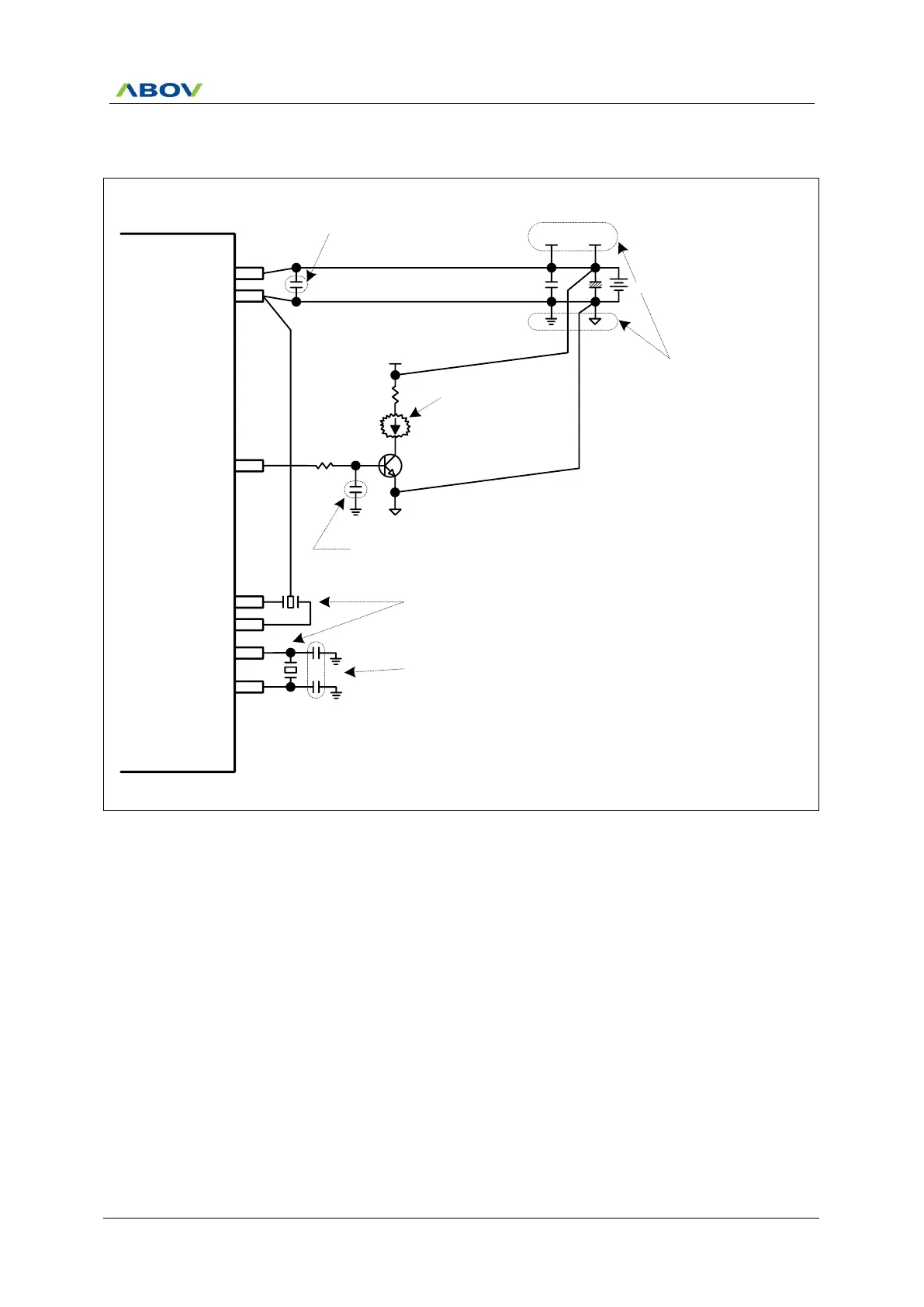
MC96F6432
XOUT
XIN
I/O
VSS
VDD
High-Current Part
Infrared LED,
FND(7-Segment),
,,,,,
etc
{ }
0.01uF
VCC
0.1uF
This 0.1uF capacitor should be within
1cm from the VDD pin of MCU on the
PCB layout.
{ }
This 0.01uF capacitor is alternatively
for noise immunity.
X-tal
SXOUT
SXIN
32.768kHz
The main and sub crystal should be
as close by the MCU as possible.
+
0.1uF
VDD VCC
{ }
The MCU power line (VDD and VSS)
should be separated from the high-
current part at a DC power node on
the PCB layout.
DC Power
The load capacitors of the sub clock
- C1, C2: CL x 2 ± 15%
- CL = (C1 x C2)/(C1 + C2) - Cstray
- CL: the specific capacitor value of crystal
- Cstray: the parasitic capacitor of a PCB (1pF – 1.5pF)
C1
C2
Figure 7.15 Recommended Circuit and Layout