MC96F6432
50 June 22, 2018 Ver. 2.9
7.18 Sub Clock Oscillator Characteristics
Table 7-18 Sub Clock Oscillator Characteristics
(T
A
= -40°C ~ +85°C, VDD= 1.8V ~ 5.5V)
Sub oscillation frequency
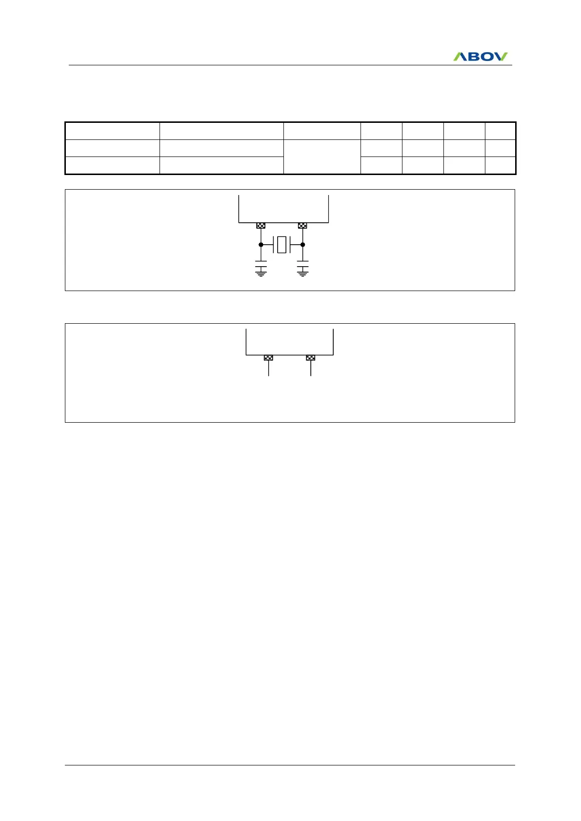
Figure 7.10 Crystal Oscillator
SXIN SXOUT
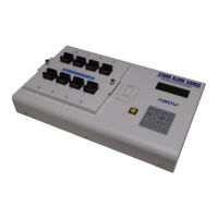
External
Clock
Source
Open
Figure 7.11 External Clock