MC96F6432
262 June 22, 2018 Ver. 2.9
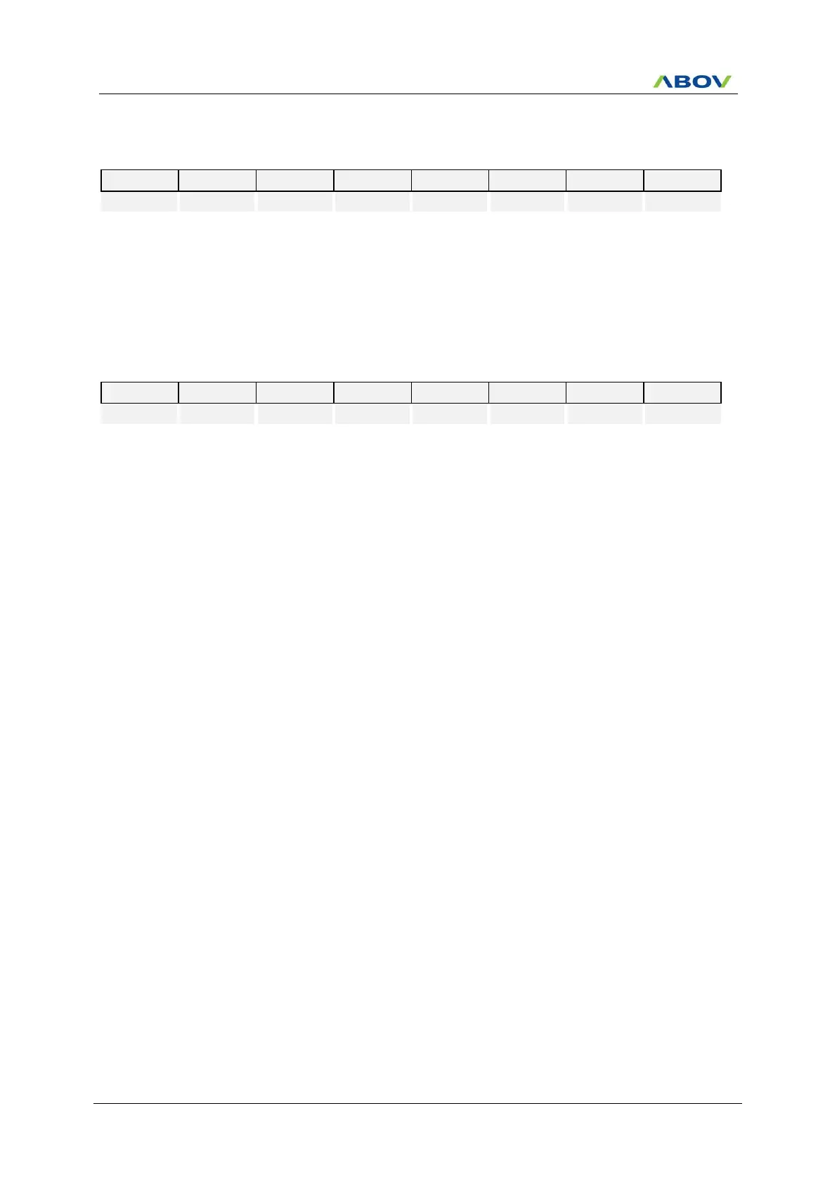
USI1SCLR (USI1 SCL Low Period Register: For I2C mode) : F6H
Initial value : 3FH
This register defines the high period of SCL1 when it operates in
I2C master mode.
The base clock is SCLK, the system clock, and the period is
calculated by the formula: t
SCLK
X (4 X USI1SCLR +2) where
t
SCLK
is the period of SCLK.
USI1SAR (USI1 Slave Address Register: For I2C mode) : EDH
Initial value : 00H
These bits configure the slave address of I2C when it operates in
I2C slave mode.
This bit decides whether I2C allows general call address or not in
I2C slave mode.
Ignore general call address
Allow general call address
 Loading...