Description of fields within Sub-Register 0x2D:06 – OTP_CTRL
This bit forces a load of LDE microcode. The LDE algorithm is responsible for generating an
accurate RX timestamp and calculating some signal quality statistics related to the received
packet. See Register file: 0x2E – Leading Edge Detection Interface for more details about the
LDE functionality. The LDE algorithm is implemented in a microcode that is stored in a special
ROM area on the DW1000 but run from a RAM area. After powering up the DW1000 (or after
exiting SLEEP or DEEPSLEEP states) the LDE RAM is empty. Before the LDE is run the code has
to be copied from ROM to RAM. This should be done before receiver is enabled if it is
important to timestamp this received frame. Set LDELOAD to 1 to initiate the loading, it will
automatically clear when the load is done. If the LDE code is not being loaded before the
receiver is enabled then the LDERUNE (LDE run enable) control in Sub-Register 0x36:04 –
PMSC_CTRL1 must be turned off (set to zero).
When waking up from SLEEP or DEEPSLEEP to receive a frame, if the ONW_LLDE bit (in Sub-
Register 0x2C:00 – AON_WCFG), has been configured to 1, then the LDE load will be done
automatically as part of exiting the sleep state.
7.2.46.4 Sub-Register 0x2D:08 – OTP_STAT
Register file: 0x2D – OTP Memory Interface, sub-register 0x08 is a 16-bit register used to give status
information about the progress of the OTP programming activity. The OTP_STAT register contains the
following fields:
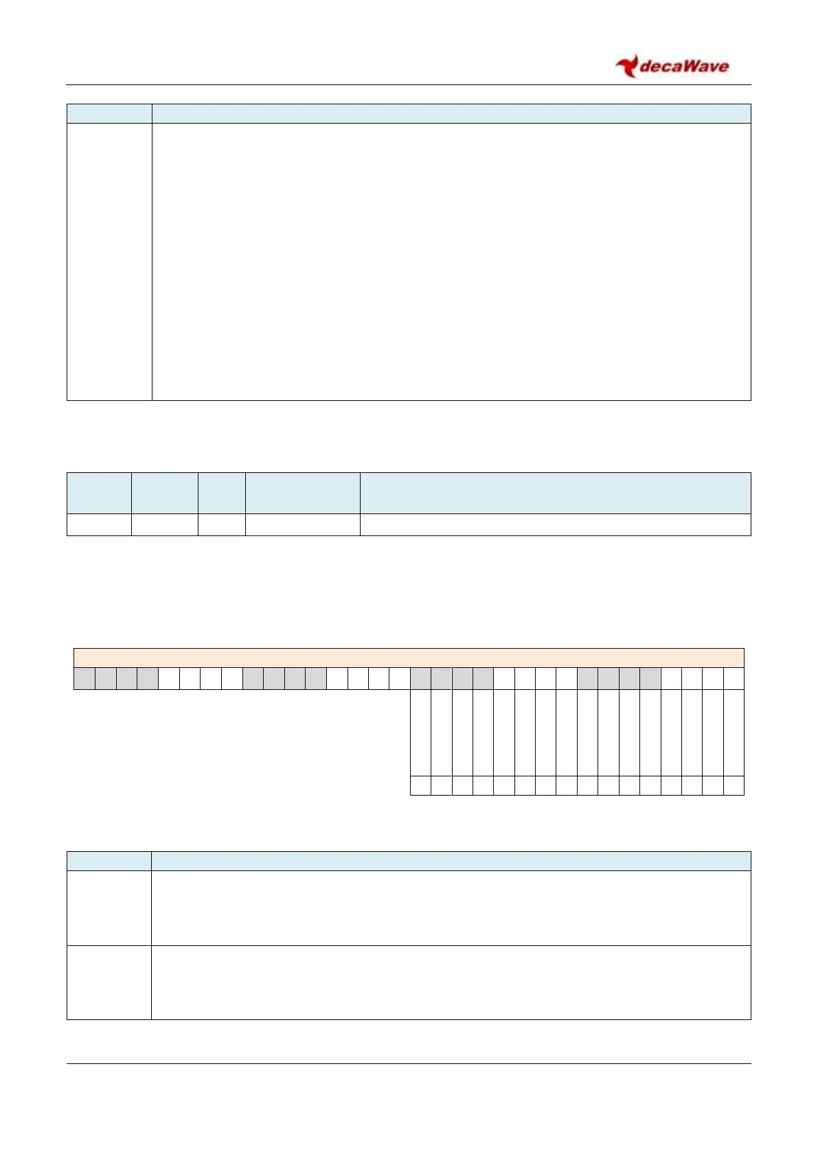
REG:2D:08 – OTP_STAT – OTP Status
The fields of the OTP_STAT register are described below:
Description of fields within Sub-Register 0x2D:08 – OTP_STAT
OTP Programming Done. This status bit indicates that the programming of the 32-bit word
from OTP_WDAT to the address specified by OTP_ADDR has completed. Writing to OTP
memory is an involved procedure. For details of this please refer to section 6.3.2 –
Programming a value into OTP memory.
OTP Programming Voltage OK. This status bit indicates that the VPP level is sufficient for
programming the OTP memory. For details of OTP programming please refer to section 6.3 –
Using the on-chip OTP memory.


 To Next Page