Reference Manual Preliminary
Prox–DU & Prox–SU
www.gemalto.com Release for first samples Do not use for final design
DOC118569A Public Use Page 124/134
conditions of the blocks.
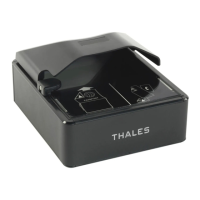
MIFARE
®
UL Memory Mapping
The MIFARE
®
Ultralight chip is a 512-bit EEPROM memory card.
The MIFARE
®
UL memory is organized in 16 pages with 4 bytes each as depicted in the
following table:
Byte Number 0 1 2 3 Page Block
Serial Number SN0 SN1 SN2 BCC0 0
Serial Number SN3 SN4 SN5 SN6 1
Internal/Lock BCC1 Internal Lock0 Lock1 2
OTP OTP0 OTP1 OTP2 OTP3 3
0
Data Read-Write Data0 Data1 Data2 Data3 4
Data Read-Write Data4 Data5 Data6 Data7 5
Data Read-Write Data8 Data9 Data10 Data11 6
Data Read-Write Data12 Data13 Data14 Data15 7
1
Data Read-Write Data16 Data17 Data18 Data19 8
Data Read-Write Data20 Data21 Data22 Data23 9
Data Read-Write Data24 Data25 Data26 Data27 10
Data Read-Write Data28 Data29 Data30 Data31 11
2
Data Read-Write Data32 Data33 Data34 Data35 12
Data Read-Write Data36 Data37 Data38 Data39 13
Data Read-Write Data40 Data41 Data42 Data43 14
Data Read-Write Data44 Data45 Data46 Data47 15
3
Bold frame indicates user area.
Table 58 – Memory mapping of MIFARE
®
UL
Serial Number Area
SN0-SN7 is the 7 bytes serial number according to ISO14443-3.
BCC0 and BCC1 are the check bytes according to ISO14443-3.
Internal byte is reserved for internal data.
These 10 bytes are write-protected after having been programmed by the chip manufacturer
after production.