AFL-HM55 Series Panel PC
Page 28
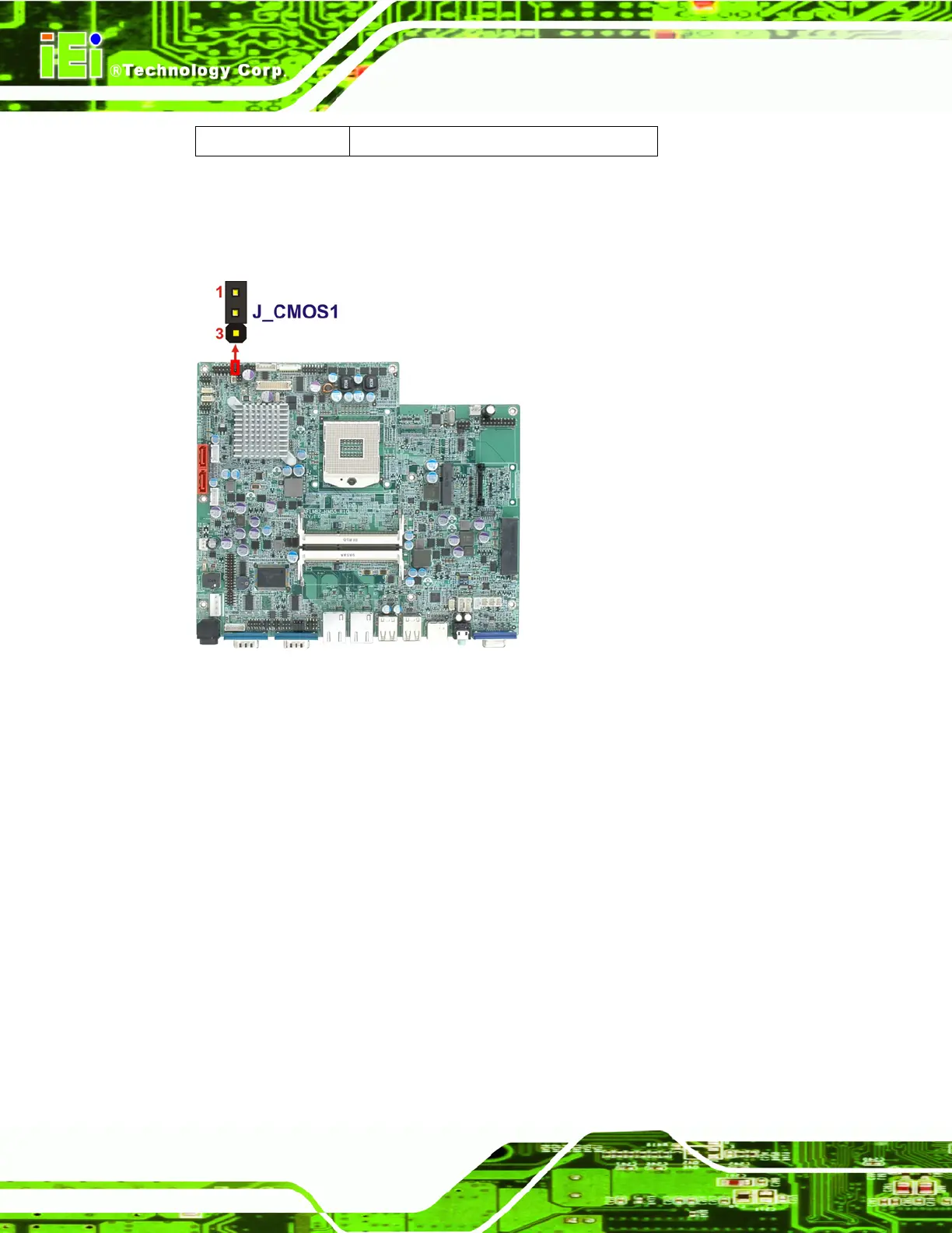
Short 2 - 3 Clear CMOS Setup
Table 3-3: Clear CMOS Jumper Settings
The location of the clear CMOS jumper is shown in Figure 3-6 below.
Figure 3-6: Clear CMOS Jumper
3.9.4 COM1 Pin 9 Setting
Jumper Label:
JP7 and JP8
Jumper Type:
6-pin header
Jumper Settings:
See Table 3-4 and Table 3-5
Jumper Loc
ation:
See Figure 3-7 and Figu
re 3-8
Two jumpers (JP7 and JP8) configure pin 9 on COM1 and COM3 DB-9 connectors. Pin 9
on the COM1 and the COM3 DB-9 connectors can be set as the ring (RI) signal, +5 V or
+12 V. The COM1 and COM3 Pin 9 Setting jumper selection options are shown in the
tables below.

 Loading...