You can use the PFL II IP core to either program the flash memory devices, configure your FPGA, or both. To perform both
functions, create separate PFL II functions if any of the following conditions apply to your design:
• You modify the flash data infrequently.
• You have JTAG or In-System Programming (ISP) access to the configuration host.
• You want to program the flash memory device with non-Intel FPGA data, for example initialization storage for an ASSP.
You can use the PFL II IP core to program the flash memory device for the following purposes:
— To write the initialization data
— To store your design source code to implement the read and initialization control with the host logic
3.1.7.3.2. Mapping PFL II IP Core and Flash Address
The address connections between the PFL II IP core and the flash memory device vary depending on the flash memory device
vendor and data bus width.
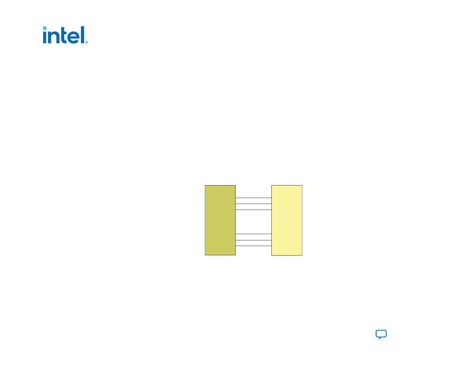
Figure 28. Flash Memory in 8-Bit Mode
The address connection between the PFL II IP core and the flash memory device are the same.
23
22
21
-
-
-
2
1
0
PFL II
23
22
21
-
-
-
2
1
0
Flash Memory
address: 24 bits address: 24 bits
3. Intel Agilex Configuration Schemes
683673 | 2021.10.29
Intel
®
Agilex
™
Configuration User Guide
Send Feedback
84
 Loading...