The BTS communicates over the JTAG bus to a test design running in the FPGA. The
Board Test System and Power Monitor share the JTAG bus with other applications like
the Nios II debugger and the Signal Tap Logic Analyzer. Because the Quartus Prime
programmer uses most of the bandwidth of the JTAG bus, other applications using the
JTAG bus might time out. Be sure to close the other applications before attempting to
reconfigure the FPGA using the Quartus Prime Programmer.
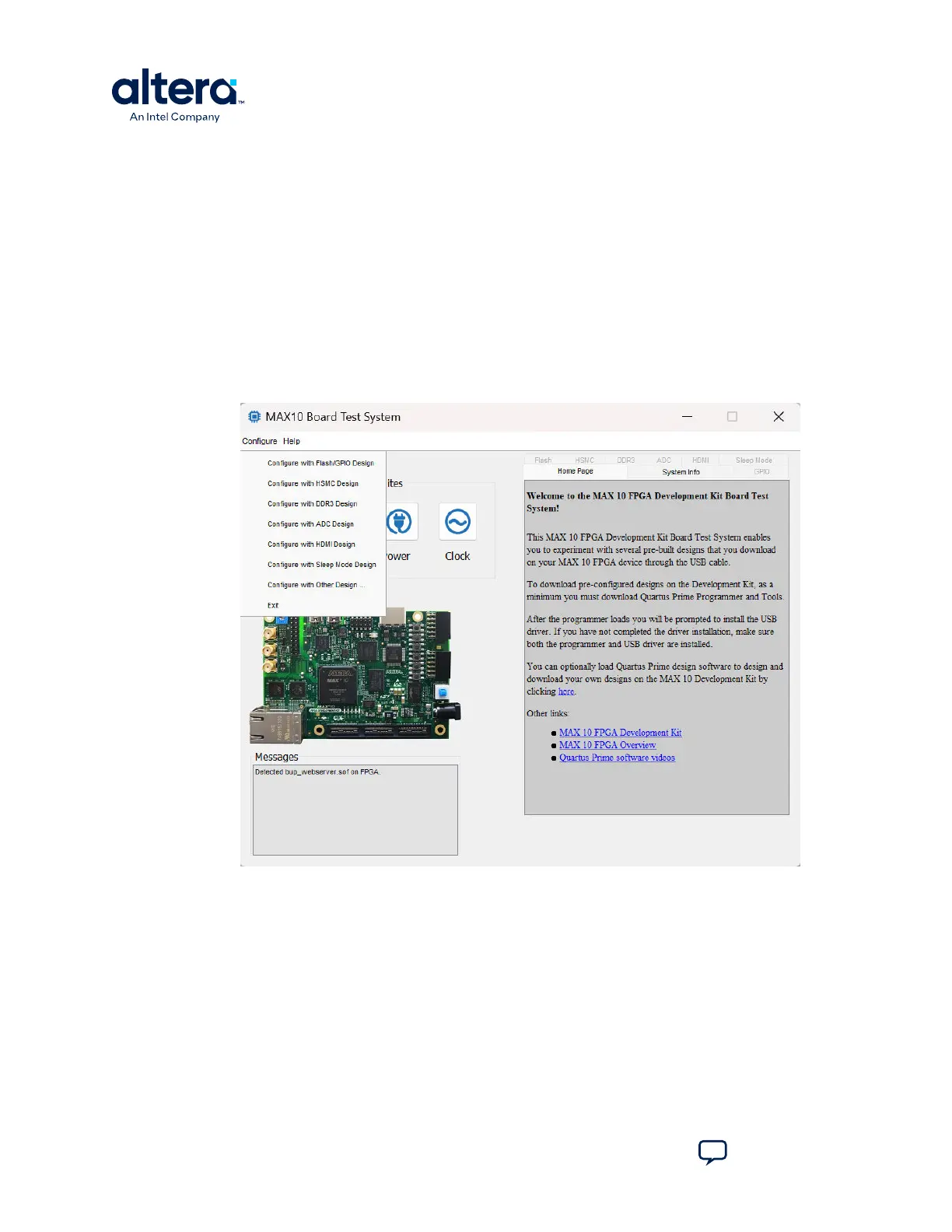
3.1. Using the Configure Menu
Use the Configure menu to select the design you want to use. Each design example
tests different board features. Choose a design from this menu and the corresponding
tabs become active for testing.
Figure 6. The Configure Menu
To configure the FPGA with a test system design, perform the following steps:
1. On the Configure menu, click the configure command that corresponds to the
functionality you want to test.
2. In the dialog box that appears, click Configure to download the corresponding
design to the FPGA.
3. When configuration finishes, close the Quartus Prime Programmer if open. The
design begins running in the FPGA. The corresponding GUI application tabs that
interface with the design are now enabled.
If you use the Quartus Prime Programmer for configuration, rather than the Board Test
System GUI, you may need to restart the GUI.
3. Board Test System
683460 | 2024.11.20
MAX
®
10 FPGA Development Kit User Guide
Send Feedback
14