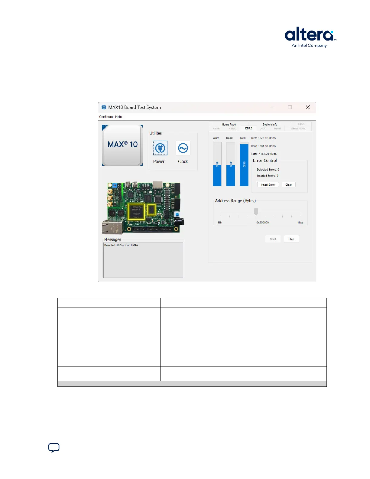
3.6. The DDR3 Tab
The DDR3 tab allows you to test the DDR3 by reading and writing to a selected
amount of addresses.
Figure 11. The DDR3 Tab
Table 7. Controls on the DDR3 Tab
Control Description
Performance Indicators These controls display current transaction performance analysis
information collected since you last clicked Start:
• Write, Read, and Total performance bars—Show the percentage of
maximum theoretical data rate that the requested transactions are able
to achieve.
• Write (MBps), Read (MBps), and Total (MBps)—Show the number
of bytes of data analyzed per second.
• Data bus: 72 bits (8 bits ECC) wide and the frequency is 1066 MHz
double data rate. 2133 Megabits per second (Mbps) per pin. Equating
to a theoretical maximum bandwidth of 136512 Mbps or 17064 MBps.
Error Control This control displays data errors detected during analysis and allows you to
insert errors:
continued...
3. Board Test System
683460 | 2024.11.20
Send Feedback
MAX
®
10 FPGA Development Kit User Guide
21