Schematic Signal Name Schematic Share Bus
Signal Name
I/O Standard MAX 10
FPGA Pin
Number
Description
PMODA_D6 PMODA_IO6
3.3 V A5 In/Out
PMODA_D7 PMODA_IO7
3.3 V E9 In/Out
—
VCC
3.3 V — Power
—
GND
— — Ground
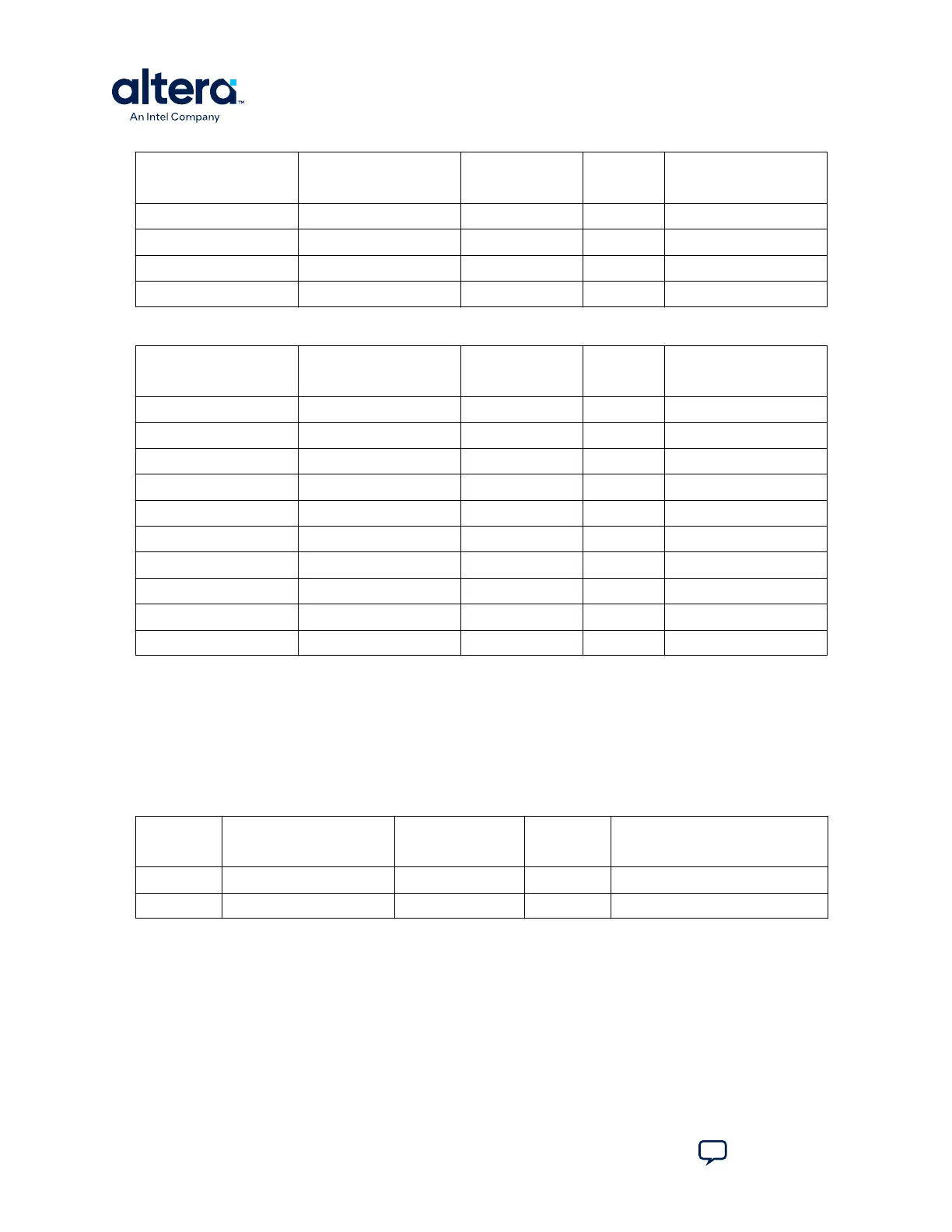
Table 33. Pmod B Pin Assignments, Signal Names, and Functions
Schematic Signal Name Schematic Share Bus
Signal Name
I/O Standard MAX 10
FPGA Pin
Number
Description
PMODB_D0 PMODB_IO0
3.3 V E8 In/Out
PMODB_D1 PMODB_IO1
3.3 V D5 In/Out
PMODB_D2 PMODB_IO2
3.3 V B5 In/Out
PMODB_D3 PMODB_IO3
3.3 V C4 In/Out
PMODB_D4 PMODB_IO4
3.3 V A2 In/Out
PMODB_D5 PMODB_IO5
3.3 V A3 In/Out
PMODB_D6 PMODB_IO6
3.3 V B4 In/Out
PMODB_D7 PMODB_IO7
3.3 V B3 In/Out
—
VCC
3.3 V — Power
—
GND
— — Ground
A.8.6. USB to UART
The board uses a USB based UART bridge chip (FT232R) to bridge communication to a
host for general software debug for Nios and non-Nios systems. This chip uses TXD
and RXD for transmission and reception of data. A mini B plug receptacle is used to
minimize board space. The related I/O utilization is implemented in Bank 4.
Table 34. USB-UART Pin Assignments, Signal Names, and Functions
Board
Reference
(U11)
Schematic Signal Name I/O Standard MAX 10
FPGA Pin
Number
Description
U11.2
UART_TX
2.5 V W18 Transmit asynchronous data output
U11.30
UART_RX
2.5 V Y19 Receive asynchronous data input
A. Development Kit Components
683460 | 2024.11.20
MAX
®
10 FPGA Development Kit User Guide
Send Feedback
54