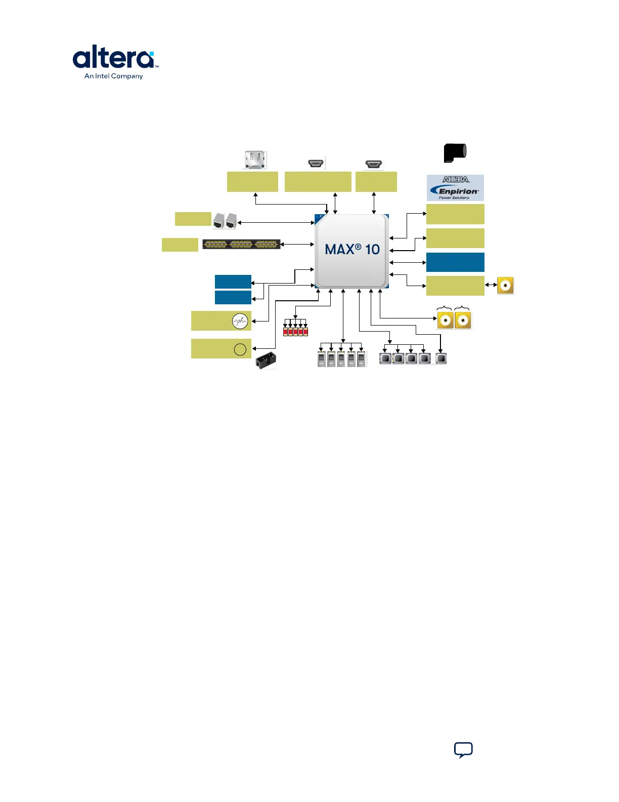
1.1. Block Diagram
Figure 3. MAX 10 FPGA Development Kit Block Diagram
~
HDMI TX
FTDI + MAX II/V
USB to UART
DC Supply
DDR 3
512 Mb x16
QSPI Flash
1 Gb x16
2x10
ADC IN/GPIO
DACOUT
DAC
AIN1
AIN2
FPGA_RESET
JTAG
Oscillator
Potentiometer
PMOD
PMOD
HSMC
2x 1 GbE
~
Intel® FPGA Download Cable
User DIP Switches
User Push Buttons
User LEDs
1.2. Feature Summary
The MAX 10 FPGA Development Kit includes a RoHS- and CE-compliant MAX 10 FPGA
development board with the following components:
Featured Devices
• MAX 10 FPGA (10M50D, dual supply, F484 package)
• Enpirion
®
EN2342QI 4 A PowerSoC Voltage-Mode Synchronous Step-Down
Converter with Integrated Inductor Enpirion
• EN6337QI 3 A High-Efficiency PowerSoC DC-DC Step-Down Converters with
Integrated Inductor
• Enpirion EP5358xUI 600 mA PowerSoC DC-DC Step-Down Converters with
Integrated Inductor
• MAX II CPLD – EPM1270M256C4N (On-board Intel
®
FPGA Download Cable II)
Programming and Configuration
• Embedded Intel FPGA Download Cable II (JTAG)
• Optional JTAG direct via 10-pin header
Memory Devices
• 64-Mx16 1 Gb DDR3 SDRAM with soft memory controller
• 128-Mx8 1 Gb DDR3 SDRAM with soft memory controller
• 512-Mb Quad serial peripheral interface (quad SPI) flash
1. Overview
683460 | 2024.11.20
MAX
®
10 FPGA Development Kit User Guide
Send Feedback
6