Board Reference
(U5 & U6)
Schematic Signal Name I/O Standard MAX 10
FPGA Pin
Number
Description
U6.E7
DDR3_DQ23
1.5 V SSTL P20 Data bus byte lane 2
U5.F3
DDR3_DQS_P0
Differential 1.5 V
SSTL
K14 Data strobe P byte lane 0
U5.G3
DDR3_DQS_N0
Differential 1.5 V
SSTL
K15 Data strobe N byte lane 0
U5.C7
DDR3_DQS_P1
Differential 1.5 V
SSTL
L14 Data strobe P byte lane 1
U5.B7
DDR3_DQS_N1
Differential 1.5 V
SSTL
L15 Data strobe N byte lane 1
U6.C3
DDR3_DQS_P2
Differential 1.5 V
SSTL
R18 Data strobe P byte lane 2
U6.D3
DDR3_DQS_N2
Differential 1.5 V
SSTL
P18 Data strobe N byte lane 2
U5.K1 - U6.G1
DDR3_ODT
1.5 V SSTL W19 On-die termination enable
U5.J3 - U6.F3
DDR3_RASn
1.5 V SSTL V18 Row address select
U5.T2 - U6.N2
DDR3_RESETn
1.5 V SSTL B22 Reset
U5.L3 - U6.H3
DDR3_WEn
1.5 V SSTL Y21 Write enable
U5.L8
DDR3_ZQ1
1.5 V SSTL — ZQ impedance calibration
U6.H8
DDR3_ZQ2
1.5 V SSTL — ZQ impedance calibration
Related Information
Block Diagram on page 6
A.9.2. DDR3 Rev. C Board
Note: For your board's revision, look for the board serial number at the bottom of the board.
Refer to the Components in MAX 10 FPGA Development Kit (Bottom View) figure for
more information.
The MAX 10 FPGA provides full-speed support to a x16 DDR3 300 MHz interface by
using a 1 Gbit x16 memory. Additionally, the MAX 10 supports the error correction
code (ECC) feature.
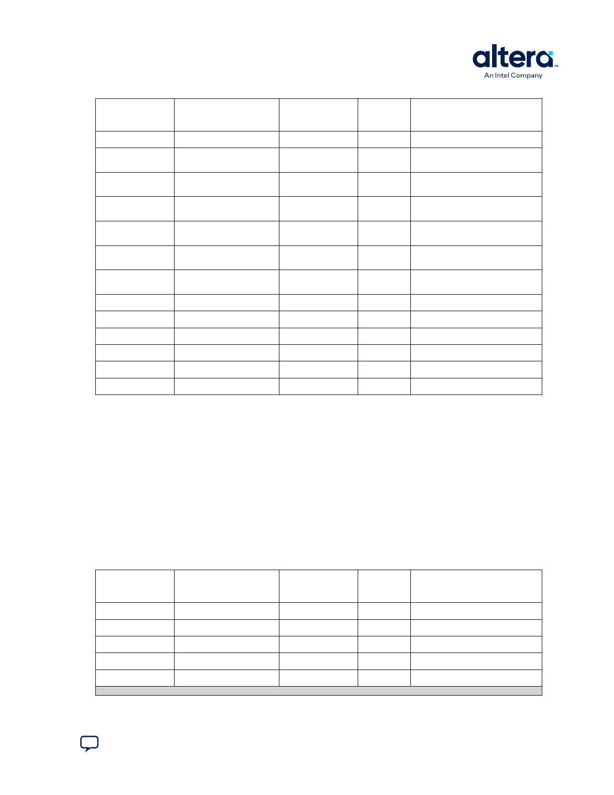
Table 36. DDR3 Pin Assignments, Signal Names, and Functions
Board Reference
(U5 & U6)
Schematic Signal Name I/O Standard MAX 10
FPGA Pin
Number
Description
U5.N3 - U6.K3
DDR3_A0
1.5 V SSTL V20 Address bus
U5.P7 - U6.L7
DDR3_A1
1.5 V SSTL D19 Address bus
U5.P3 - U6.L3
DDR3_A2
1.5 V SSTL A21 Address bus
U5.N2 - U6.K2
DDR3_A3
1.5 V SSTL U20 Address bus
U5.P8 - U6.L8
DDR3_A4
1.5 V SSTL C20 Address bus
continued...
A. Development Kit Components
683460 | 2024.11.20
Send Feedback
MAX
®
10 FPGA Development Kit User Guide
57