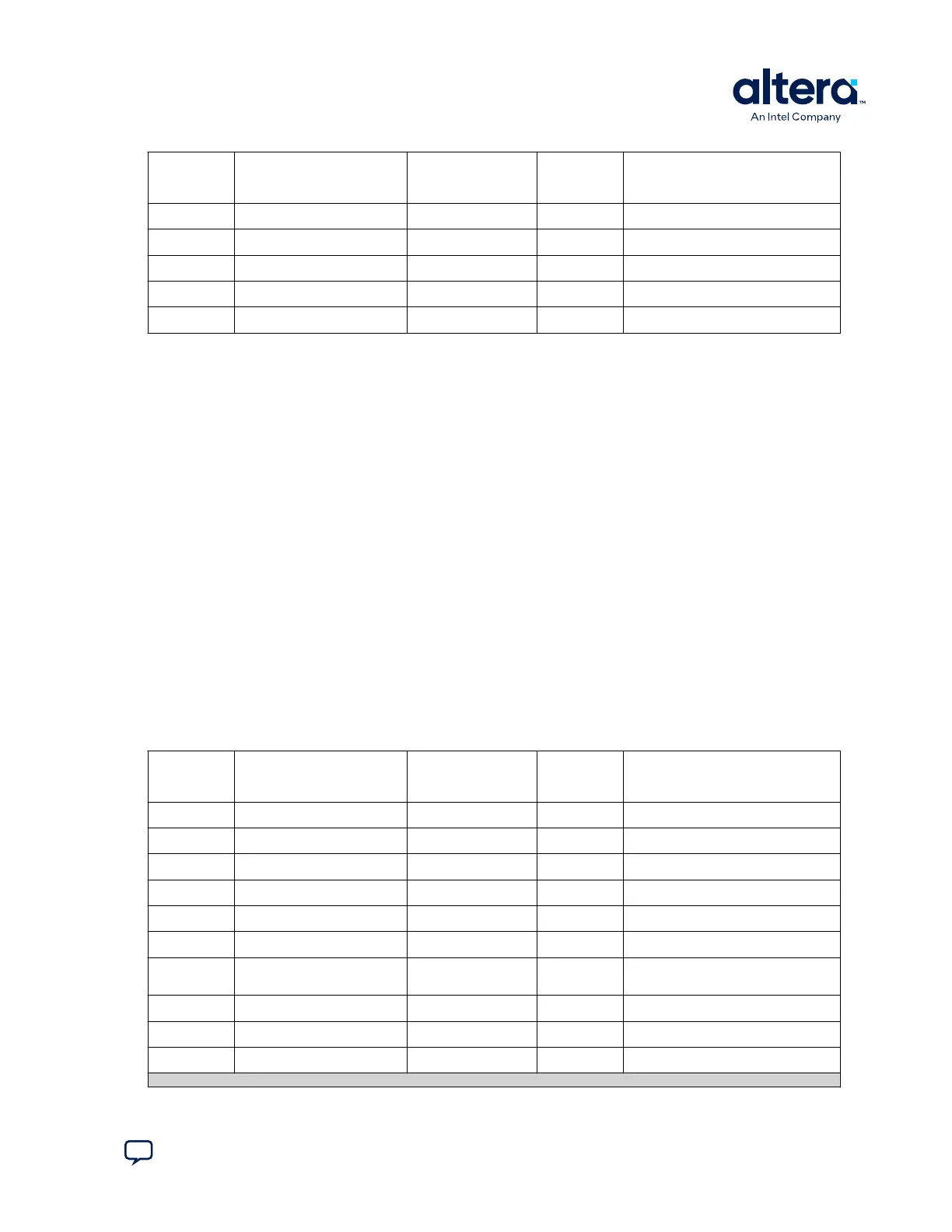
Board
Reference
(U8)
Schematic Signal Name I/O Standard MAX 10
FPGA Pin
Number
Description
U8.64
HDMI_TX_HS
3.3 V A19 Vertical Synchronization
U8.2
HDMI_TX_VS
3.3 V J12 Horizontal Synchronization
U8.28
HDMI_TX_INT
3.3 V D15 Interrupt Signal
U8.35
HDMI_SCL
3.3 V A10 HDMI I2C clock
U8.36
HDMI_SDAX
3.3 V B15 HDMI I2C data
A.8.4. HSMC
The high-speed mezzanine card (HSMC) interface is based on the Samtec 0.5 mm
pitch, surface-mount QTH/QSH family of connectors. It is designed to support a full
SPI-4.2 interface (17 LVDS channels) and 3 input and output clocks as well as SMBus
and JTAG signals.
Since MAX 10 does not have transceiver channels, the HSMC clock-data-recovery
channels are left unconnected.
The HSMC interface has programmable bi-directional I/O pins that can be used as 2.5
V LVCMOS, which is 3.3-V LVTTL-compatible. These pins can also be used as various
differential I/O standards including, but not limited to, LVDS, mini-LVDS, and RSDS
with up to 17 full-duplex channels.
As noted in the High Speed Mezzanine Card (HSMC) Specification manual, LVDS and
single-ended I/O standards are only guaranteed to function when mixed according to
either the generic single-ended pin-out or generic differential pin-out.
For more information about the HSMC specification such as signaling standards, signal
integrity, compatible connectors, and mechanical information, refer to the High Speed
Mezzanine Card (HSMC) Specification manual.
Table 31. HSMC Schematic Signals
Board
Reference
(J2)
Schematic Signal Name I/O Standard MAX
10/MAX II
Pin Number
Description
33
HSMC_SDA
2.5 V CMOS inout AA19 Management serial data line
34
HSMC_SCL
2.5 V CMOS out Y18 Management serial clock line
35
HSMC_JTAG_TCK
Part of chain A9 (MAX II) JTAG clock
36
HSMC_JTAG_TMS
Part of chain A8 (MAX II) JTAG mode select
37
HSMC_JTAG_TDO
Part of chain A7 (MAX II) JTAG data out
38
HSMC_JTAG_TDI
Part of chain A6 (MAX II) JTAG data in
39
HSMC_CLK_OUT0
2.5 V CMOS clock
output
AA13 clock output 0
40
HSMC_CLK_IN0
2.5 V CMOS clock in N4 Clock input 0
41
HSMC_D0
2.5 V CMOS inout Y7 Data bus
42
HSMC_D1
2.5 V CMOS inout Y8 Data bus
continued...
A. Development Kit Components
683460 | 2024.11.20
Send Feedback
MAX
®
10 FPGA Development Kit User Guide
49