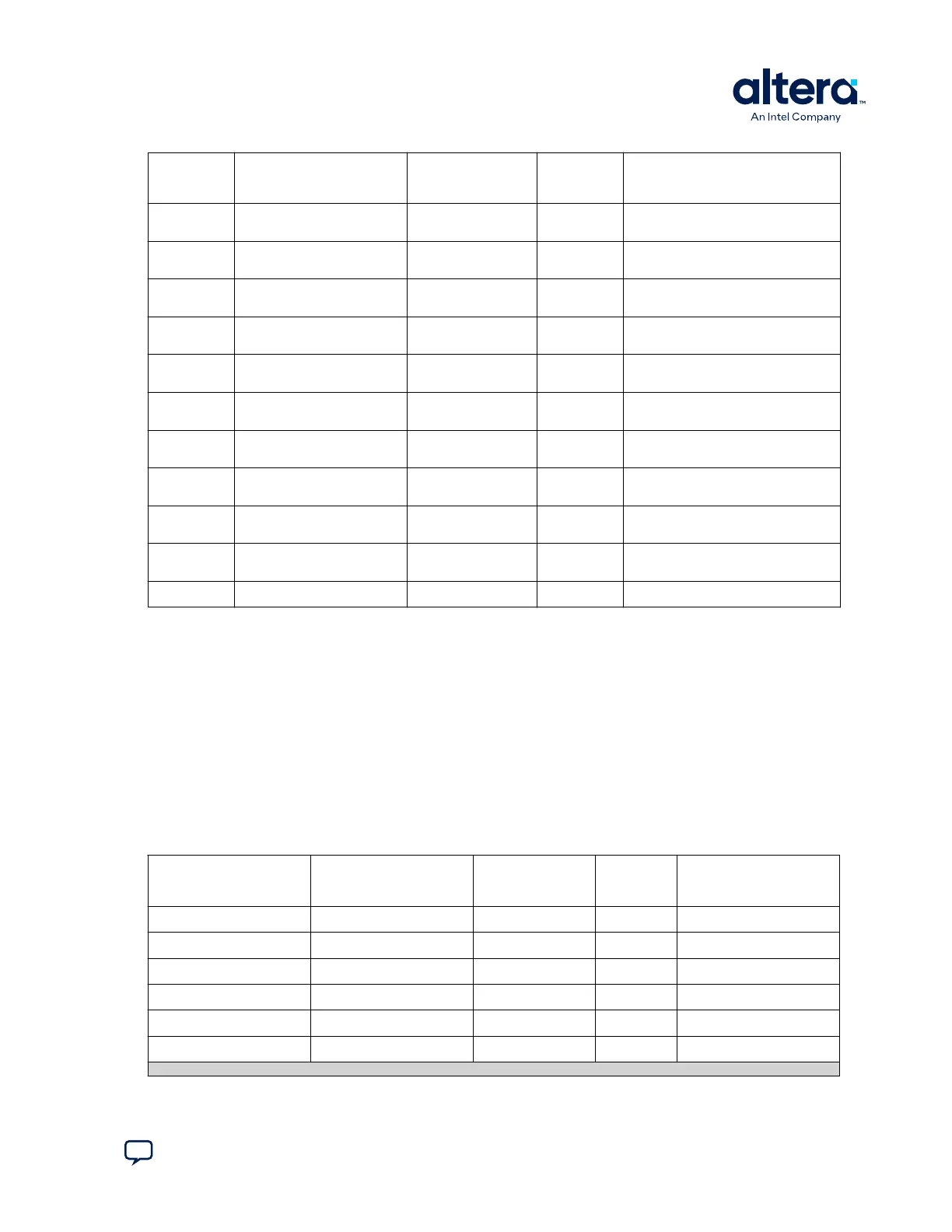
Board
Reference
(J2)
Schematic Signal Name I/O Standard MAX
10/MAX II
Pin Number
Description
145
HSMC_TX_D_N15
2.5 V CMOS inout or
LVDS TX channels-n
AA11 Data bus
146
HSMC_RX_D_N15
(1)
2.5 V CMOS inout or
LVDS RX channels-n
AB12 Data bus
149
HSMC_TX_D_P16
2.5 V CMOS inout or
LVDS TX channels-p
Y17 Data bus
150
HSMC_RX_D_P16
(1)
2.5 V CMOS inout or
LVDS RX channels-p
AB20 Data bus
151
HSMC_TX_D_N16
2.5 V CMOS inout or
LVDS TX channels-n
AA17 Data bus
152
HSMC_RX_D_N16
(1)
2.5 V CMOS inout or
LVDS RX channels-n
AB19 Data bus
155
HSMC_CLK_OUT_P2
2.5 V CMOS inout or
LVDS clock out
W15 Clock output 2
156
HSMC_CLK_IN_P2
2.5 V CMOS inout or
LVDS clock in
V10 Clock input 2
157
HSMC_CLK_OUT_N2
2.5 V CMOS inout or
LVDS clock out
V14 Clock output 2
158
HSMC_CLK_IN_N2
2.5 V CMOS inout or
LVDS clock in
V9 Clock input 2
160
HSMC_PRSNTn
2.5 V AB14 Present
Related Information
High Speed Mezzanine Card (HSMC) Specification
A.8.5. Pmod Connectors
The MAX 10 FPGA Development Kit features two Digilent Pmod* compatible headers,
which are used to connect low frequency, low I/O pin count peripheral modules.
The 12-pin version Pmod connector used in this kit provides 8 I/O signal pins. The
peripheral module interface also encompasses a variant using I
2
C interface, and two
or four wire MTE cables. The Pmod signals are connected to Bank 8.
Table 32. Pmod A Pin Assignments, Signal Names, and Functions
Schematic Signal Name Schematic Share Bus
Signal Name
I/O Standard MAX 10
FPGA Pin
Number
Description
PMODA_D0 PMODA_IO0
3.3 V C7 In/Out
PMODA_D1 PMODA_IO1
3.3 V C8 In/Out
PMODA_D2 PMODA_IO2
3.3 V A6 In/Out
PMODA_D3 PMODA_IO3
3.3 V B7 In/Out
PMODA_D4 PMODA_IO4
3.3 V D8 In/Out
PMODA_D5 PMODA_IO5
3.3 V A4 In/Out
continued...
A. Development Kit Components
683460 | 2024.11.20
Send Feedback
MAX
®
10 FPGA Development Kit User Guide
53