A.9. Memory
This section describes the development board's memory interface support and also
their signal names, types, and connectivity relative to the FPGA.
A.9.1. DDR3 Rev. B Board
Note: For your board's revision, look for the board serial number on the back of the board at
the bottom. Refer to the Components in MAX 10 FPGA Development Kit (Bottom View)
figure for more information.
The MAX 10 FPGA provides full-speed support to a x16 DDR3 300-MHz interface by
using a 1 Gbit x16 memory. Additionally, the MAX 10 supports the error correction
code (ECC) feature.
Caution: The DDR3 address signals at F18, E19, F20, and F21 on Rev. B boards violate MAX 10
external memory guidelines when implementing DDR3 on the 10M50 F484 device.
Altera recommends you follow the MAX 10 guidelines for your own board designs and
utilize Quartus Prime software to verify pin location compliance. Contact Altera support
if you received DDR3 pin location errors for your Rev. B kit designs.
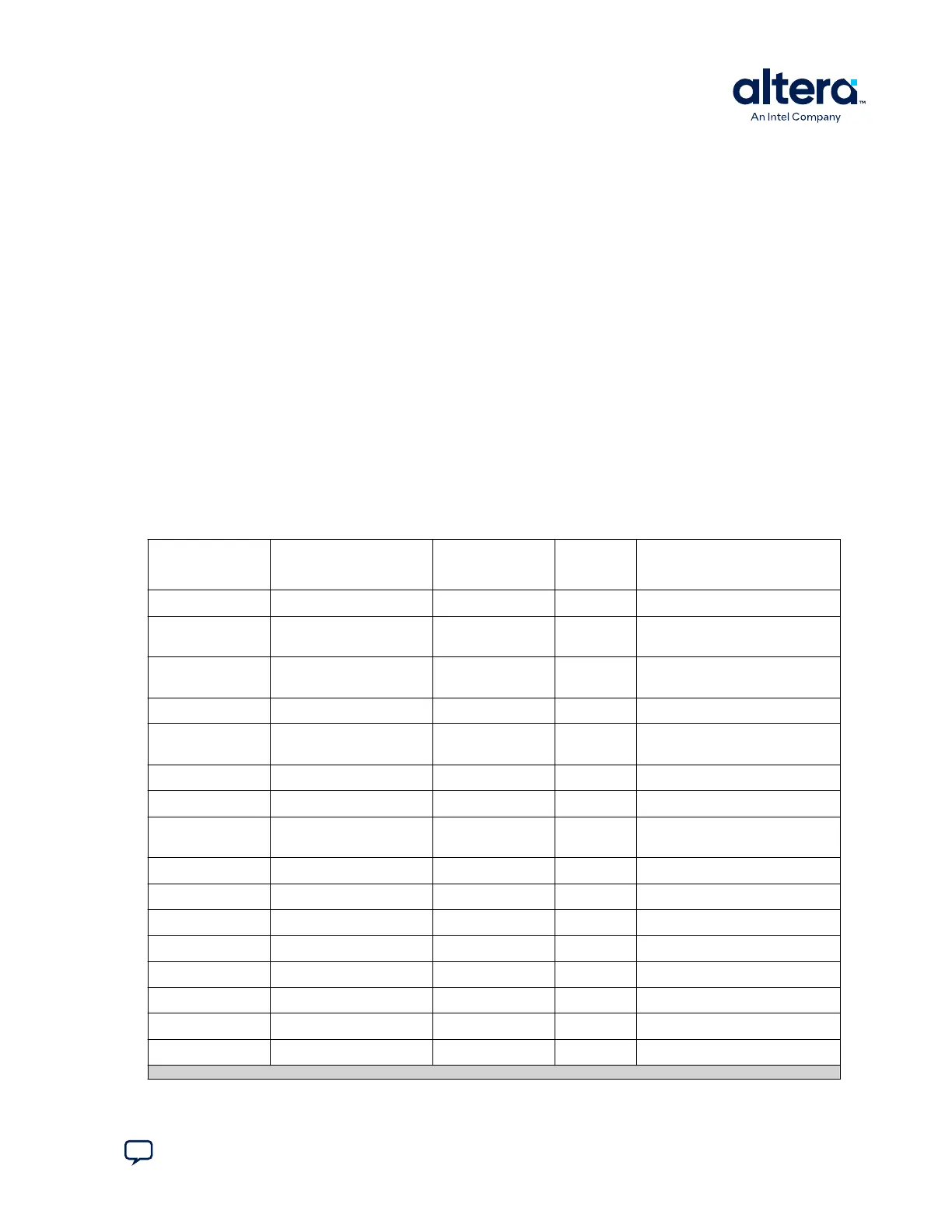
Table 35. DDR3 Pin Assignments, Signal Names, and Functions
Board Reference
(U5 & U6)
Schematic Signal Name I/O Standard MAX 10
FPGA Pin
Number
Description
U5.N3 - U6.K3
DDR3_A0
1.5 V SSTL V20 Address bus
U5.P7 - U6.L7
DDR3_A1
1.5 V SSTL F20 Address bus
Refer to Caution statement above.
U5.P3 - U6.L3
DDR3_A2
1.5 V SSTL F18 Address bus
Refer to Caution statement above.
U5.N2 - U6.K2
DDR3_A3
1.5 V SSTL U20 Address bus
U5.P8 - U6.L8
DDR3_A4
1.5 V SSTL F21 Address bus
Refer to Caution statement above.
U5.P2 - U6.L2
DDR3_A5
1.5 V SSTL F19 Address bus
U5.R8 - U6.M8
DDR3_A6
1.5 V SSTL E21 Address bus
U5.R2 -U6.M2
DDR3_A7
1.5 V SSTL E19 Address bus
Refer to Caution statement above.
U5.T8 - U6.N8
DDR3_A8
1.5 V SSTL D22 Address bus
U5.R3 - U6.M3
DDR3_A9
1.5 V SSTL E22 Address bus
U5.L7 - U6.H7
DDR3_A10
1.5 V SSTL Y20 Address bus
U5.R7 - U6.M7
DDR3_A11
1.5 V SSTL E20 Address bus
U5.N7 - U6.K7
DDR3_A12
1.5 V SSTL J14 Address bus
U5.T3 - U6.N3
DDR3_A13
1.5 V SSTL C22 Address bus
U5.M2 - U6.J2
DDR3_BA0
1.5 V SSTL V22 Bank address bus
U5.N8 - U6.K8
DDR3_BA1
1.5 V SSTL N18 Bank address bus
continued...
A. Development Kit Components
683460 | 2024.11.20
Send Feedback
MAX
®
10 FPGA Development Kit User Guide
55