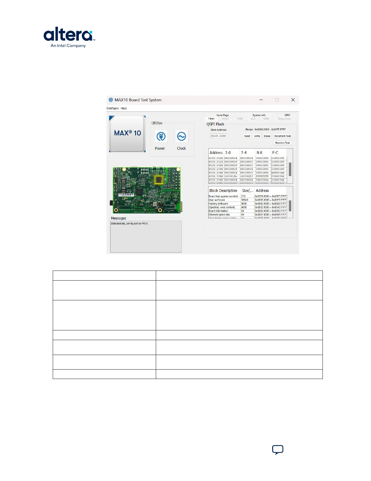
3.4. The Flash Tab
The Flash tab allows you to read and write flash memory on your board.
Figure 9. The Flash Tab (Detail)
Table 5. Controls on the Flash Tab
Control Description
Read Reads the flash memory on your board. To see the flash memory contents,
type a starting address in the text box and click Read. Values starting at
the specified address appear in the table.
Write Writes the flash memory on your board. To update the flash memory
contents, change values in the table and click Write. The application writes
the new values to flash memory and then reads the values back to
guarantee that the graphical display accurately reflects the memory
contents.
Erase Erases flash memory.
Increment Test Starts an incrementing data pattern test to flash memory, limited to the
512 K test system scratch page.
Random Test Starts a random data pattern test to flash memory, limited to the 512 K
test system scratch page.
Flash Memory Map Displays the flash memory map for the development board.
3. Board Test System
683460 | 2024.11.20
MAX
®
10 FPGA Development Kit User Guide
Send Feedback
18