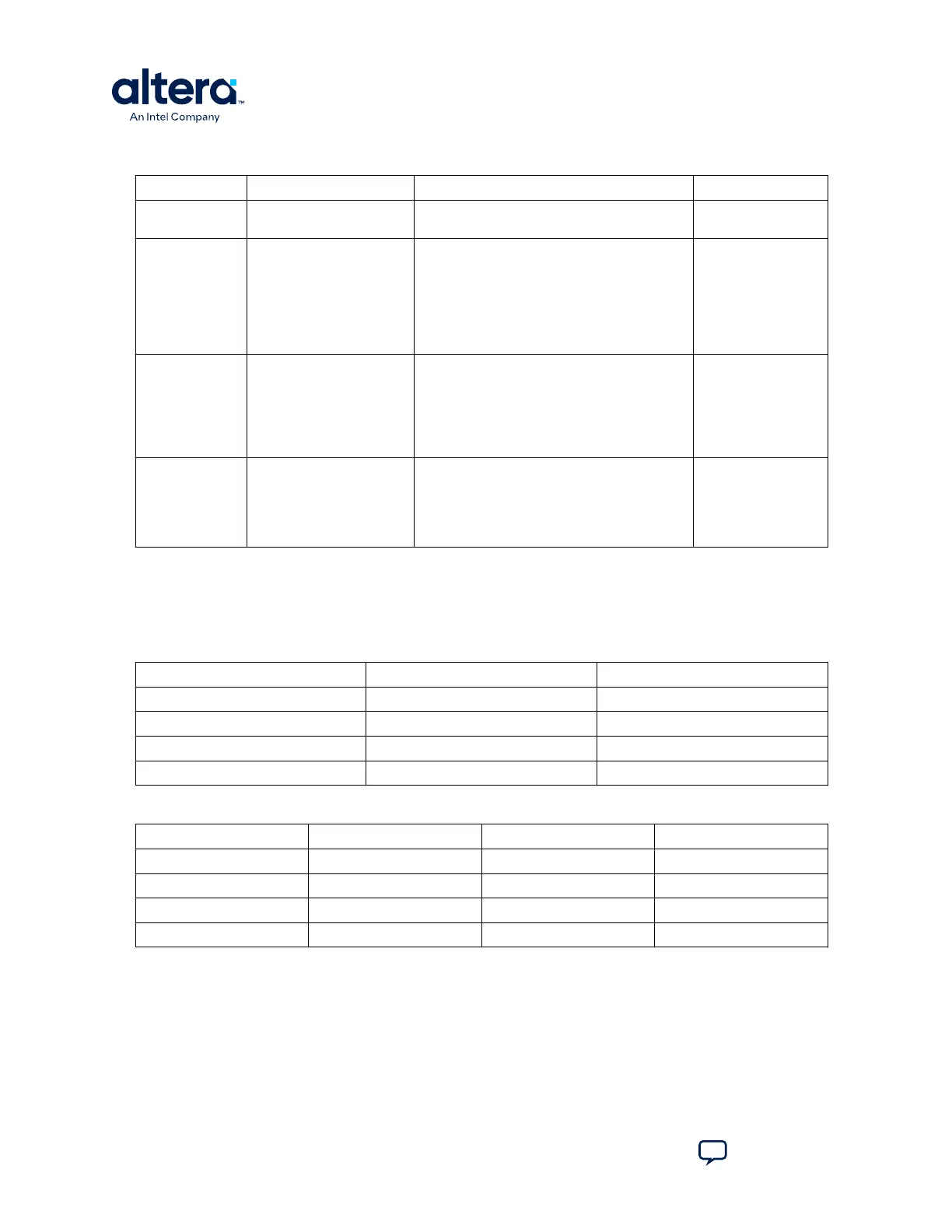
Table 16. SW2 DIP Switch Settings (Board Bottom)
Switch Board Label Function Default Position
1 USER_DIPSW4 User defined switch #4, #0/1/2/3 is on SW1.
No default function.
—
2 BOOT_SEL (for Rev. B
Board)
CONFIG_SEL (for Rev. C
board)
Use this pin to choose CFM0, CFM1 or CFM2
image as the first boot image in dual-image
configuration. If the CONFIG_SEL is set to low,
the first boot image is CFM0 image. If the
CONFIG_SEL pin is set to high, the first boot
image is CFM1 or CFM2 image. This pin is read
before user mode and before the nSTATUS pin
is asserted.
LOW
3 VTAP_BYPASSN A virtual JTAG device is provided within the On-
Board Intel FPGA Download Cable II, it provides
access to diagnostic hardware and board
identification information. The device shows up
as an extra device on the JTAG chain with ID:
020D10DD. This switch removes the virtual
JTAG device from the JTAG chain.
HIGH
4 HSMC_BYPASSN Use this pin to bypass HSMC from JTAG chain.
The default value of this signal is high so HSMC
is in the JTAG chain. (However, there is no
daughter cards connected to HSMC normally so
it would not be detected by JTAG master).
When it is set to low, HSMC is bypassed.
HIGH
A.4. Status Elements
This topic lists the non-user status elements for the MAX 10 FPGA development board.
Table 17. General LED Signal Names
Board Reference Signal Name Description
D1 — Blue Power LED
D2 HSMC_PRSNTn Green LED
D13 UART_TXLED Green LED for USB to UART
D14 UART_RXLED Green LED for USB to UART
Table 18. MAX II CPLD LED Signal Names
Board Reference Signal Name I/O Standard MAX II CPLD Pin Number
D20 MAXII_CONF_DONE 3.3 V W17
D21 3.3V_LED 3.3 V U4
D22 2.5V_LED 3.3 V U5
D23 1.2V_LED 3.3 V U6
A. Development Kit Components
683460 | 2024.11.20
MAX
®
10 FPGA Development Kit User Guide
Send Feedback
40