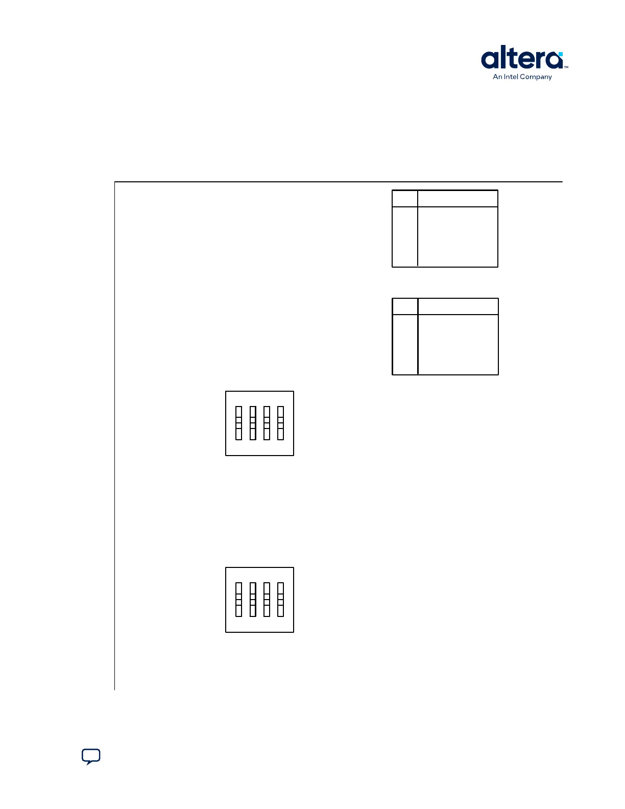
Figure 21. Switches on the Bottom Board (Detail)
When a switch is ON, it means the FUNCTION SIGNAL is connected to GND. So it is a LOGIC LOW (0). When
switch is OFF, it means the FUNCTION SIGNAL is disconnected from GND. So it is a LOGIC HIGH (1).
Note: The following figure shows the switch labels for the Rev. C board and a note for the Rev. B board. The change
of name for SW2.3 is just a name change, not a functional change. Rev. B is labeled MAX10_BYPASS, but it is
actually a VTAP bypass.
4 3 2 1
OFF = 1
For Rev. B:
2 = BOOT_SEL
3 = MAX10_BYPASSN
OFF = 1
ON = 0
ON = 0
SW2
SW1
1 2 3 4
SW1
1
2
3
4
FUNCTION
USER_DIPSW0
USER_DIPSW1
USER_DIPSW2
USER_DIPSW3
SW2
1
2
3
4
FUNCTION
USER_DIPSW4
CONFIG_SEL
VTAP_BYPASSN
HSMC_BYPASSN
A. Development Kit Components
683460 | 2024.11.20
Send Feedback
MAX
®
10 FPGA Development Kit User Guide
39