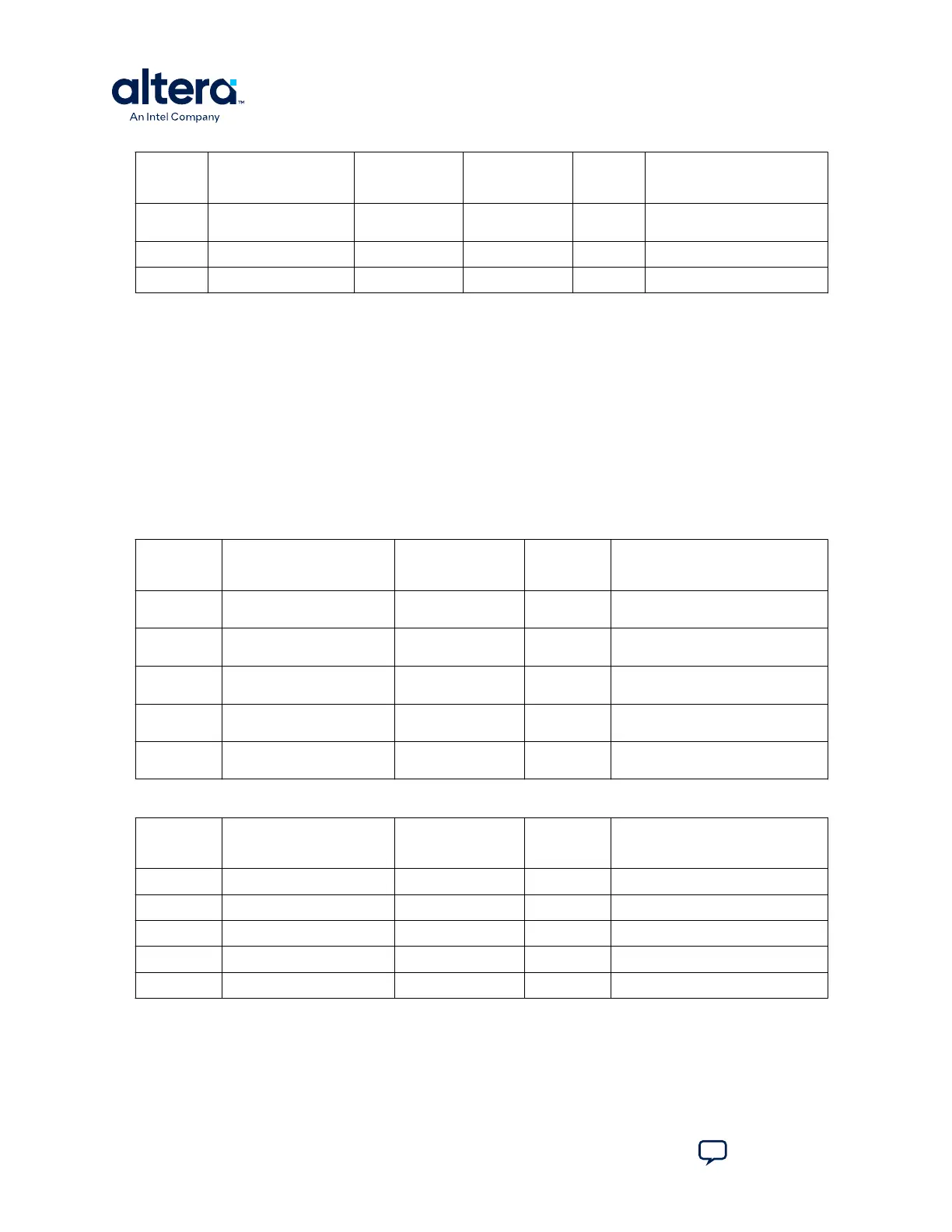
Source Schematic Signal
Name
Frequency
(MHz)
I/O Standard MAX 10
FPGA Pin
Number
Application
U2
CLK_DDR3_100_P
100.000 Differential
SSTL-15
N14 DDR3 clocks
U2
CLK_LVDS_125_N
125.000 2.5 V LVDS R11 LVDS clocks
U2
CLK_LVDS_125_P
125.000 2.5 V LVDS P11 LVDS clocks
Note: For signal CLK_50_MAXII, the output side voltage is 2.5 V and the input side voltage
is 3.3 V. However, they are compatible electrically.
Note:
For signals CLK_DDR3_100_P and CLK_DDR3_100_N, at the MAX 10 input side,
Differential SSTL-15 is used as I/O standard because this bank's VCCIO is 1.5 V.
A.7.2. Off-Board Clock Input/Output
The development board has input and output clocks which can be driven onto the
board. The output clocks can be programmed to different levels and I/O standards
according to the FPGA device’s specification.
Table 25. Off-Board Clock Inputs
Source Schematic Signal Name I/O Standard MAX 10
FPGA Pin
Number
Description
HSMC
HSMC_CLK_IN_N1
2.5 V AB21 LVDS input from the installed HSMC
cable or board.
HSMC
HSMC_CLK_IN_P1
2.5 V AA20 LVDS input from the installed HSMC
cable or board.
HSMC
HSMC_CLK_IN_N2
2.5 V V9 LVDS input from the installed HSMC
cable or board.
HSMC
HSMC_CLK_IN_P2
2.5 V V10 LVDS input from the installed HSMC
cable or board.
HSMC
HSMC_CLK_IN0
2.5 V N4 Single-ended input from the
installed HSMC cable or board.
Table 26. Off-Board Clock Outputs
Source Schematic Signal Name I/O Standard MAX 10
FPGA Pin
Number
Description
HSMC
HSMC_CLK_OUT_N1
2.5 V R13 LVDS output
HSMC
HSMC_CLK_OUT_P1
2.5 V P13 LVDS output
HSMC
HSMC_CLK_OUT_N2
2.5 V V14 LVDS output
HSMC
HSMC_CLK_OUT_P2
2.5 V W15 LVDS output
HSMC
HSMC_CLK_OUT0
2.5 V AA13 FPGA CMOS output (or GPIO)
A. Development Kit Components
683460 | 2024.11.20
MAX
®
10 FPGA Development Kit User Guide
Send Feedback
44