• Must have a Dual Boot IP core in the design, for example, in a Platform
Designer (Standard) component.
• Choose Dual Compressed Images (512 Kbits UFM) for the
Configuration Mode.
•
Generate two .sof files above and convert them into one POF file for CFM
programming.
6. Turn on Generate compressed bitstreams, if needed.
7. Click OK.
A.3.3. Switch and Jumper Settings
This section is for the MAX 10 FPGA Development Kit. This section shows you how to
restore the default factory settings and explains their functions.
The jumper (J7) connects the output of potentiometer (POT1.2) to ADC1_CH6. When
the jumper (J7) is on, you can use the potentiometer to provide adjustable voltage
(0–2.5 V) to the MAX 10 ADC through ADC1_CH6. When the jumper (J7) is off,
ADC1_CH6 is connected to the 2x10 header as the other ADC channels.
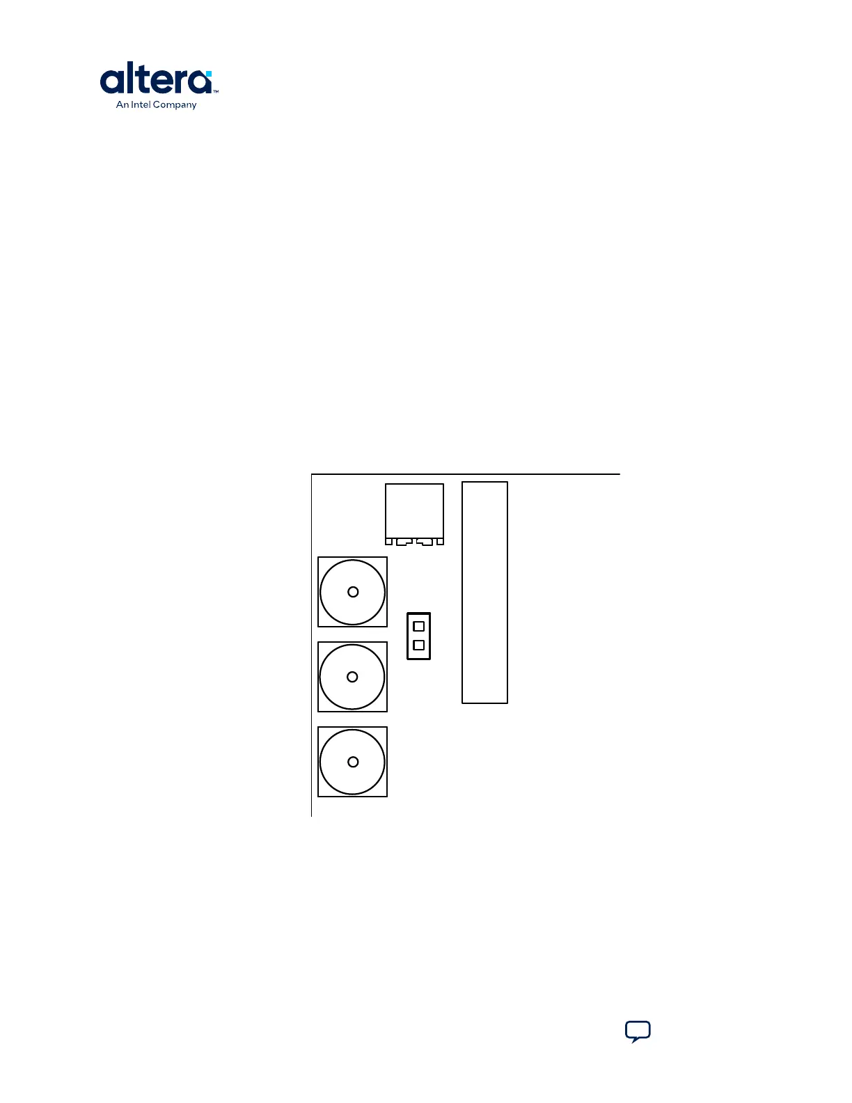
Figure 20. Jumper J7 on the Top of the Board (Detail)
J7
POT1
ANAIN1
ANAIN2
DACOUT
1
2
J20
There are two switches (SW1 and SW2) on the bottom of the board. SW1 is for user
functions, and SW2 allows for booting selection and bypassing some components.
A. Development Kit Components
683460 | 2024.11.20
MAX
®
10 FPGA Development Kit User Guide
Send Feedback
38