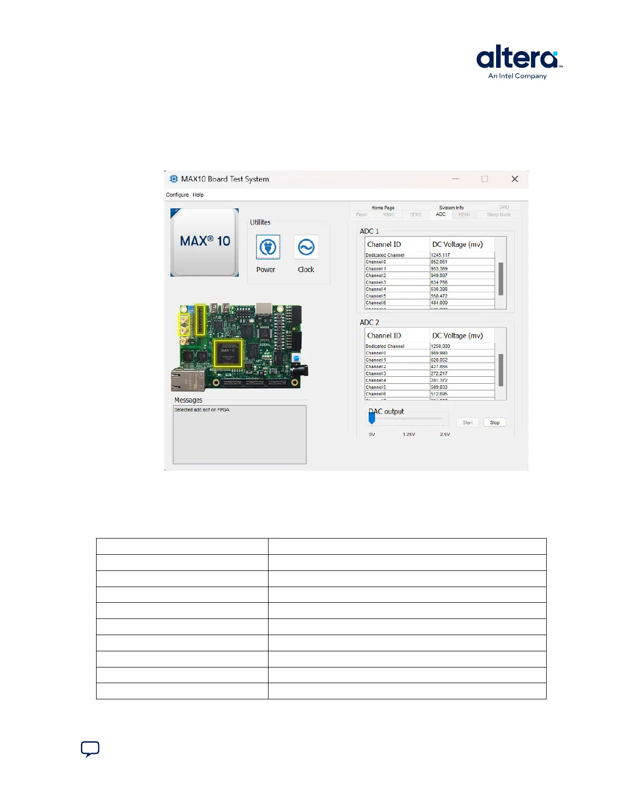
3.7. The ADC Tab
The ADC tab (analog-to-digital) shows the real-time voltage values of all of the ADC
input channels.
Figure 12. The ADC Tab
The two tables displayed on this tab, ADC 1 and ADC 2, are not editable.
The following tables show where the channels connect to.
Table 8. ADC 1 Channel Connection
Dedicated Channel SMA Connector
ADC 1 ANAIN1_SMA(J18)
Channel 0 ADC1_CH0(J20.1)
Channel 1 ADC1_CH1(J20.3)
Channel 2 ADC1_CH2(J20.5)
Channel 3 ADC1_CH2(J20.7)
Channel 4 ADC1_CH4(J20.11)
Channel 5 ADC1_CH4(J20.13)
Channel 6 ADC1_CH6(J20.15 or POT1)
Channel 7 ADC1_CH7(J20.17)
3. Board Test System
683460 | 2024.11.20
Send Feedback
MAX
®
10 FPGA Development Kit User Guide
23