Board Reference
(U5 & U6)
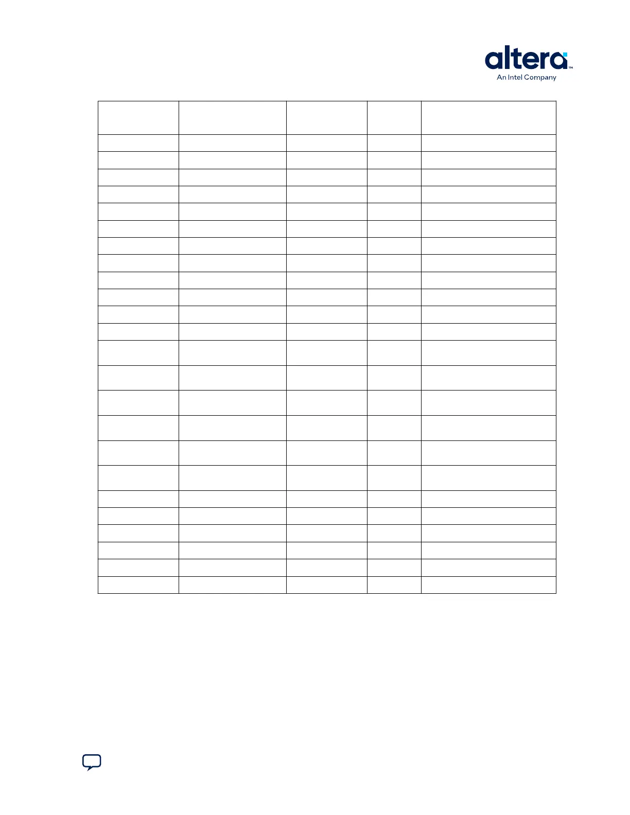
Schematic Signal Name I/O Standard MAX 10
FPGA Pin
Number
Description
U5.A7
DDR3_DQ12
1.5 V SSTL L18 Data bus byte lane 1
U5.A2
DDR3_DQ13
1.5 V SSTL M15 Data bus byte lane 1
U5.B8
DDR3_DQ14
1.5 V SSTL L19 Data bus byte lane 1
U5.A3
DDR3_DQ15
1.5 V SSTL N20 Data bus byte lane 1
U6.B3
DDR3_DQ16
1.5 V SSTL R14 Data bus byte lane 2
U6.C7
DDR3_DQ17
1.5 V SSTL P19 Data bus byte lane 2
U6.C2
DDR3_DQ18
1.5 V SSTL P14 Data bus byte lane 2
U6.C8
DDR3_DQ19
1.5 V SSTL R20 Data bus byte lane 2
U6.E3
DDR3_DQ20
1.5 V SSTL R15 Data bus byte lane 2
U6.E8
DDR3_DQ21
1.5 V SSTL T19 Data bus byte lane 2
U6.D2
DDR3_DQ22
1.5 V SSTL P15 Data bus byte lane 2
U6.E7
DDR3_DQ23
1.5 V SSTL P20 Data bus byte lane 2
U5.F3
DDR3_DQS_P0
Differential 1.5 V
SSTL
K14 Data strobe P byte lane 0
U5.G3
DDR3_DQS_N0
Differential 1.5 V
SSTL
K15 Data strobe N byte lane 0
U5.C7
DDR3_DQS_P1
Differential 1.5 V
SSTL
L14 Data strobe P byte lane 1
U5.B7
DDR3_DQS_N1
Differential 1.5 V
SSTL
L15 Data strobe N byte lane 1
U6.C3
DDR3_DQS_P2
Differential 1.5 V
SSTL
R18 Data strobe P byte lane 2
U6.D3
DDR3_DQS_N2
Differential 1.5 V
SSTL
P18 Data strobe N byte lane 2
U5.K1 - U6.G1
DDR3_ODT
1.5 V SSTL W19 On-die termination enable
U5.J3 - U6.F3
DDR3_RASn
1.5 V SSTL V18 Row address select
U5.T2 - U6.N2
DDR3_RESETn
1.5 V SSTL B22 Reset
U5.L3 - U6.H3
DDR3_WEn
1.5 V SSTL Y21 Write enable
U5.L8
DDR3_ZQ1
1.5 V SSTL — ZQ impedance calibration
U6.H8
DDR3_ZQ2
1.5 V SSTL — ZQ impedance calibration
A.9.3. Flash
The MAX 10 FPGA Development Kit provides a 512 Mb (megabit) quad SPI flash
memory. The Generic Quad SPI controller core is used by default to erase, read, and
write quad SPI flash in reference designs of the Board Test System (BTS) installer.
If you use the parallel flash loader (PFL) IP to program the quad SPI flash, you need to
generate a .pof (Programmer Object file) to configure the device.
A. Development Kit Components
683460 | 2024.11.20
Send Feedback
MAX
®
10 FPGA Development Kit User Guide
59