A.5. Setup Elements
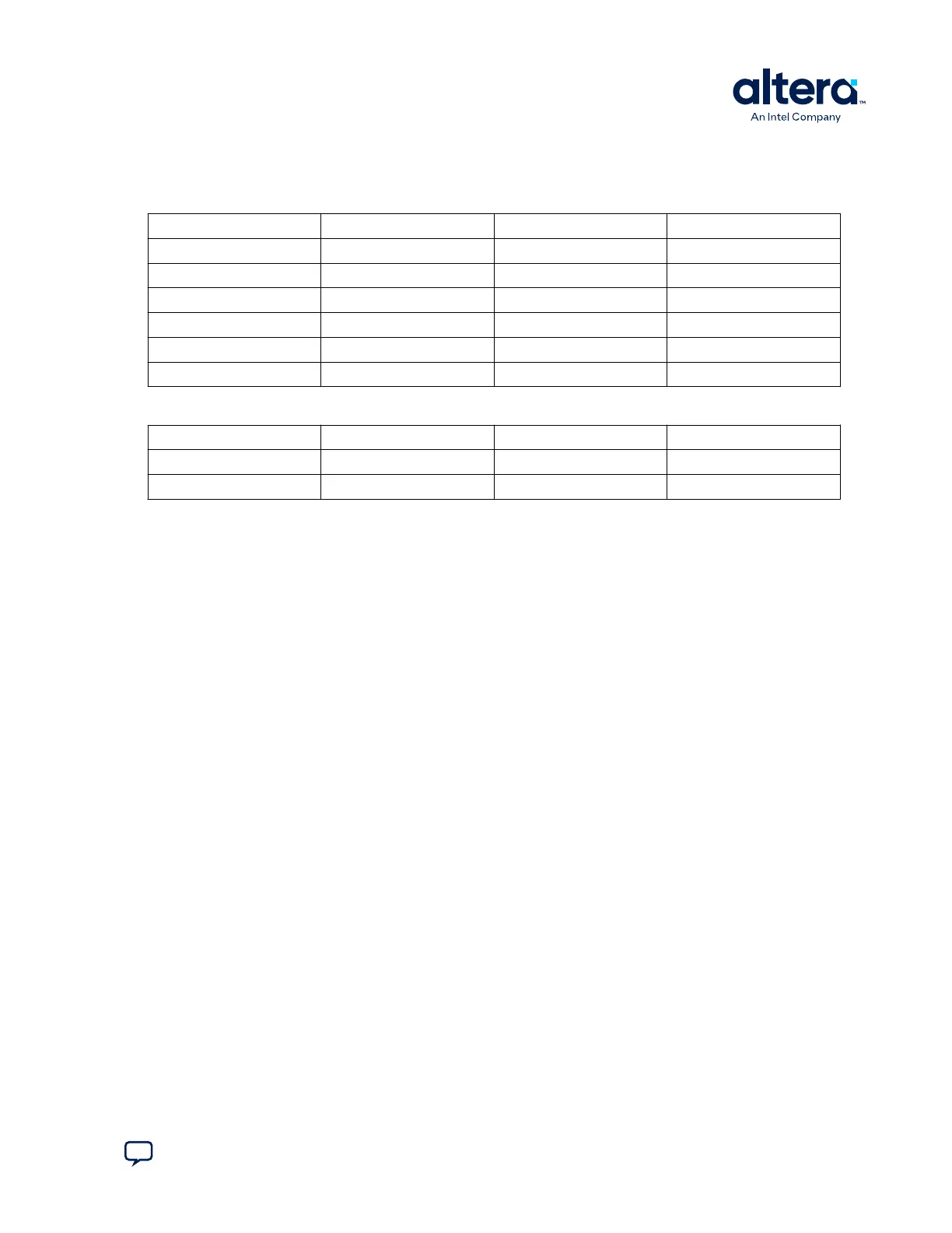
Table 19. Board Settings DIP Switch and Jumper Schematic Signals
Board Reference Signal Name Device/Pin Number I/O Standard
SW2.1 USER_DIPSW4 MAX 10 / H21 1.5 V
SW2.2 CONFIG_SEL MAX 10 / H10 3.3 V
SW2.3 VTAP_BYPASSN MAX II / P17 3.3 V
SW2.4 HSMC_BYPASSn MAX II / P18 3.3 V
J7.1 — POT1 2.5 V
J7.2 ADC1_CH6 2x10 Header / J20.15 2.5 V
Table 20. General Push Button Signal Names
Board Reference Signal Name MAX 10 FPGA Pin Number I/O Standard
S5 PULSE_NCONFIG H9 3.3 V
S6 CPU_RESETn D9 3.3 V
A. Development Kit Components
683460 | 2024.11.20
Send Feedback
MAX
®
10 FPGA Development Kit User Guide
41