A. Development Kit Components
This chapter introduces all the important components on the development kit board.
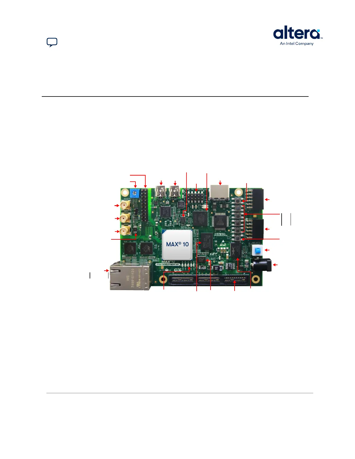
A.1. Board Overview
This section describes all the components on the development board. A complete set
of schematics, a physical layout database, and Gerber files for the development board
reside in the development kit documents directory.
Figure 18. Components in MAX 10 FPGA Development Kit (Top View)
PMOD
CONNECTOR
(J4)
FPGA
RECONFIGURE
BUTTON
USER
PUSH BUTTONS
DC INPUT
12 V
(J15)
HSMC CONNECTOR
(J2)
USER LEDs
DDR3 64Mx16
SDRAM
Enpirion EN2342QI 4A
PowerSoC
Enpirion EN6337 3A
PowerSoC
JTAG HEADER
(J14)
USB
BLASTER
(J12)
USB to UART
(J11)
CLOCK GENERATION
CHIP
POT1
2x10 PIN HEADER
(J20)
SMA - ANAIN2
(J19)
HDMI CONNECTOR
(J8)
FPGA_CPU_RESET
BUTTON
POWER
SWITCH
(SW3)
PMOD
CONNECTOR
(J5)
DUAL ETHERNET
CONNECTOR
(RJ1)
SMA - ANAIN1
(J18)
SMA - DACOUT
(J1)
16-Bit DAC
MAX II INTEL FPGA DOWNLOAD CABLE II
CIRCUIT
Ethernet A (Bottom)
Ethernet B (Top)
USER PB3
USER PB2
USER PB1
USER PB0
683460 | 2024.11.20
Send Feedback
©
Altera Corporation. Altera, the Altera logo, the ‘a’ logo, and other Altera marks are trademarks of Altera
Corporation. Altera and Intel warrant performance of its FPGA and semiconductor products to current
specifications in accordance with Altera’s or Intel's standard warranty as applicable, but reserves the right to
make changes to any products and services at any time without notice. Altera and Intel assume no
responsibility or liability arising out of the application or use of any information, product, or service described
herein except as expressly agreed to inwriting by Altera or Intel. Altera and Intel customers are advised to
obtain the latest version of device specifications before relying on any published information and before placing
orders for products or services.
*Other names and brands may be claimed as the property of others.
ISO
9001:2015
Registered