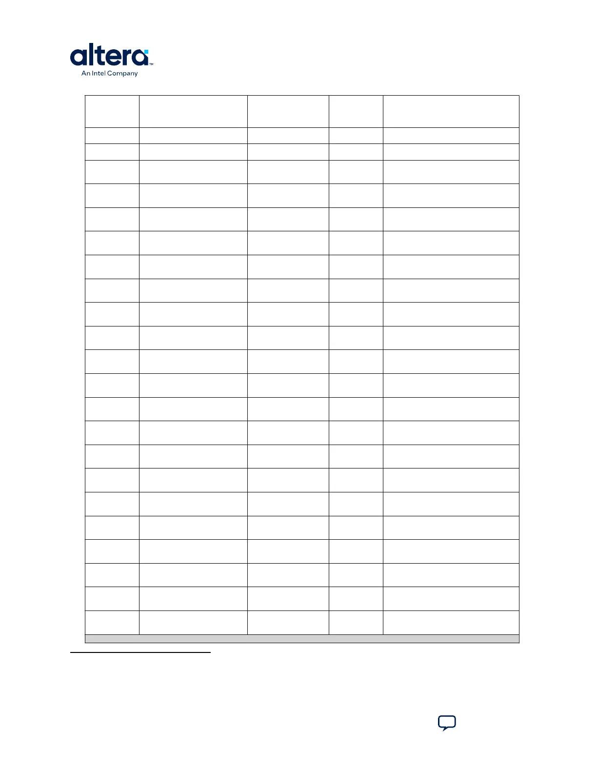
Board
Reference
(J2)
Schematic Signal Name I/O Standard MAX
10/MAX II
Pin Number
Description
43
HSMC_D2
2.5 V CMOS inout AB2 Data bus
44
HSMC_D3
2.5 V CMOS inout AB3 Data bus
47
HSMC_TX_D_P0
2.5 V CMOS inout or
LVDS TX channels-p
W3 Data bus
48
HSMC_RX_D_P0
2.5 V CMOS inout or
LVDS RX channels-p
V5 Data bus
49
HSMC_TX_D_N0
2.5 V CMOS inout or
LVDS TX channels-n
W4 Data bus
50
HSMC_RX_D_N0
(1)
2.5 V CMOS inout or
LVDS RX channels-n
V4 Data bus
53
HSMC_TX_D_P1
2.5 V CMOS inout or
LVDS TX channels-p
U7 Data bus
54
HSMC_RX_D_P1
(1)
2.5 V CMOS inout or
LVDS RX channels-p
Y2 Data bus
55
HSMC_TX_D_N1
2.5 V CMOS inout or
LVDS TX channels-n
U6 Data bus
56
HSMC_RX_D_N1
(1)
2.5 V CMOS inout or
LVDS RX channels-n
Y1 Data bus
59
HSMC_TX_D_P2
2.5 V CMOS inout or
LVDS TX channels-p
W6 Data bus
60
HSMC_RX_D_P2
(1)
2.5 V CMOS inout or
LVDS RX channels-p
AA20 Data bus
61
HSMC_TX_D_N2
2.5 V CMOS inout or
LVDS TX channels-n
W5 Data bus
62
HSMC_RX_D_N2
(1)
2.5 V CMOS inout or
LVDS RX channels-n
AA1 Data bus
65
HSMC_TX_D_P3
2.5 V CMOS inout or
LVDS TX channels-p
W8 Data bus
66
HSMC_RX_D_P3
(1)
2.5 V CMOS inout or
LVDS RX channels-p
AB8 Data bus
67
HSMC_TX_D_N3
2.5 V CMOS inout or
LVDS TX channels-n
W7 Data bus
68
HSMC_RX_D_N3
(1)
2.5 V CMOS inout or
LVDS RX channels-n
AA8 Data bus
71
HSMC_TX_D_P4
2.5 V CMOS inout or
LVDS TX channels-p
AA10 Data bus
72
HSMC_RX_D_P4
(1)
2.5 V CMOS inout or
LVDS RX channels-p
AB9 Data bus
73
HSMC_TX_D_N4
2.5 V CMOS inout or
LVDS TX channels-n
Y10 Data bus
74
HSMC_RX_D_N4
(1)
2.5 V CMOS inout or
LVDS RX channels-n
AA9 Data bus
continued...
(1)
MAX 10 does not have internal termination for LVDS RX. Install a 100 ohm resistor to support
LVDS RX on HSMC.
A. Development Kit Components
683460 | 2024.11.20
MAX
®
10 FPGA Development Kit User Guide
Send Feedback
50