Thermal/Mechanical Specifications and Design Guide 81
PECI Interface
7.1.4.9.3 Supported Responses
The typical client response is a passing FCS, a passing Completion Code and valid data.
Under some conditions, the client’s response will indicate a failure.
7.1.4.9.4 RdIAMSR() Capabilities
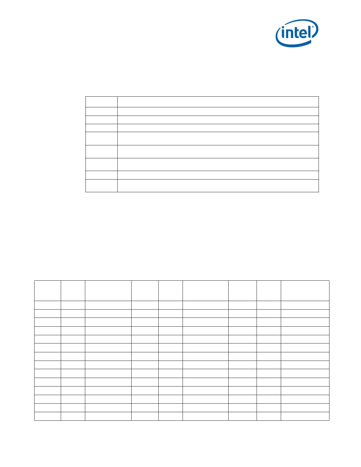
The processor PECI client allows PECI RdIAMSR() access to the registers listed in
Ta b l e 7 - 12 . These registers pertain to the processor core and uncore error banks
(machine check banks 0 through 19). Information on the exact number of accessible
banks can also be obtained by issuing a RDMSR to the IA32_MCG_CAP[7:0] MSR
(0x179). Any attempt to read processor MSRs that are not accessible over PECI or
simply not implemented will result in a completion code of 0x90.
PECI access to these registers is expected only when in-band access mechanisms are
not available.
Table 7-11. RdIAMSR() Response Definition
Response Meaning
Bad FCS Electrical error
Abort FCS Invalid command formatting (mismatched RL/WL/Command Code)
CC: 0x40 Command passed, data is valid.
CC: 0x80
Response timeout. The processor was not able to generate the required response in a timely
fashion. Retry is appropriate.
CC: 0x81
Response timeout. The processor is not able to allocate resources for servicing this command
at this time. Retry is appropriate.
CC: 0x82
The processor hardware resources required to service this command are in a low power state.
Retry may be appropriate after modification of PECI wake mode behavior if appropriate.
CC: 0x90 Unknown/Invalid Request
CC: 0x91
PECI control hardware, firmware or associated logic error. The processor is unable to process
the request.
Table 7-12. RdIAMSR() Services Summary (Sheet 1 of 2)
Processor
ID
(byte)
MSR
Address
(dword)
Meaning
Processor
ID
(byte)
MSR
Address
(dword)
Meaning
Processor
ID
(byte)
MSR
Address
(dword)
Meaning
0x0-0xF 0x0400 IA32_MC0_CTL 0x0-0xF 0x041B IA32_MC6_MISC 0x0-0xF 0x0436 IA32_MC13_ADDR
0x0-0xF 0x0280 IA32_MC0_CTL2 0x0-0xF 0x041C IA32_MC7_CTL 0x0-0xF 0x0437 IA32_MC13_MISC
0x0-0xF 0x0401 IA32_MC0_STATUS 0x0-0xF 0x0287 IA32_MC7_CTL2 0x0-0xF 0x0438 IA32_MC14_CTL
0x0-0xF 0x0402 IA32_MC0_ADDR 0x0-0xF 0x041D IA32_MC7_STATUS 0x0-0xF 0x028E IA32_MC14_CTL2
0x0-0xF 0x0403 IA32_MC0_MISC 0x0-0xF 0x041E IA32_MC7_ADDR 0x0-0xF 0x0439 IA32_MC14_STATUS
0x0-0xF 0x0404 IA32_MC1_CTL 0x0-0xF 0x041F IA32_MC7_MISC 0x0-0xF 0x043A IA32_MC14_ADDR
0x0-0xF 0x0281 IA32_MC1_CTL2 0x0-0xF 0x0420 IA32_MC8_CTL 0x0-0xF 0x043B IA32_MC14_MISC
0x0-0xF 0x0405 IA32_MC1_STATUS 0x0-0xF 0x0288 IA32_MC8_CTL2 0x0-0xF 0x043C IA32_MC15_CTL
0x0-0xF 0x0406 IA32_MC1_ADDR 0x0-0xF 0x0421 IA32_MC8_STATUS 0x0-0xF 0x028F IA32_MC15_CTL2
0x0-0xF 0x0407 IA32_MC1_MISC 0x0-0xF 0x0422 IA32_MC8_ADDR 0x0-0xF 0x043D IA32_MC15_STATUS
0x0-0xF 0x0408 IA32_MC2_CTL 0x0-0xF 0x0423 IA32_MC8_MISC 0x0-0xF 0x043E IA32_MC15_ADDR
0x0-0xF 0x0282 IA32_MC2_CTL2 0x0-0xF 0x0424 IA32_MC9_CTL 0x0-0xF 0x043F IA32_MC15_MISC
0x0-0xF 0x0409 IA32_MC2_STATUS 0x0-0xF 0x0289 IA32_MC9_CTL2 0x0-0xF 0x0440 IA32_MC16_CTL
0x0-0xF 0x040A IA32_MC2_ADDR 0x0-0xF 0x0425 IA32_MC9_STATUS 0x0-0xF 0x0290 IA32_MC16_CTL2
 Loading...