LGA2011-0 Socket
22 Thermal/Mechanical Specifications and Design Guide
3.1 Contact/Land Mating Location
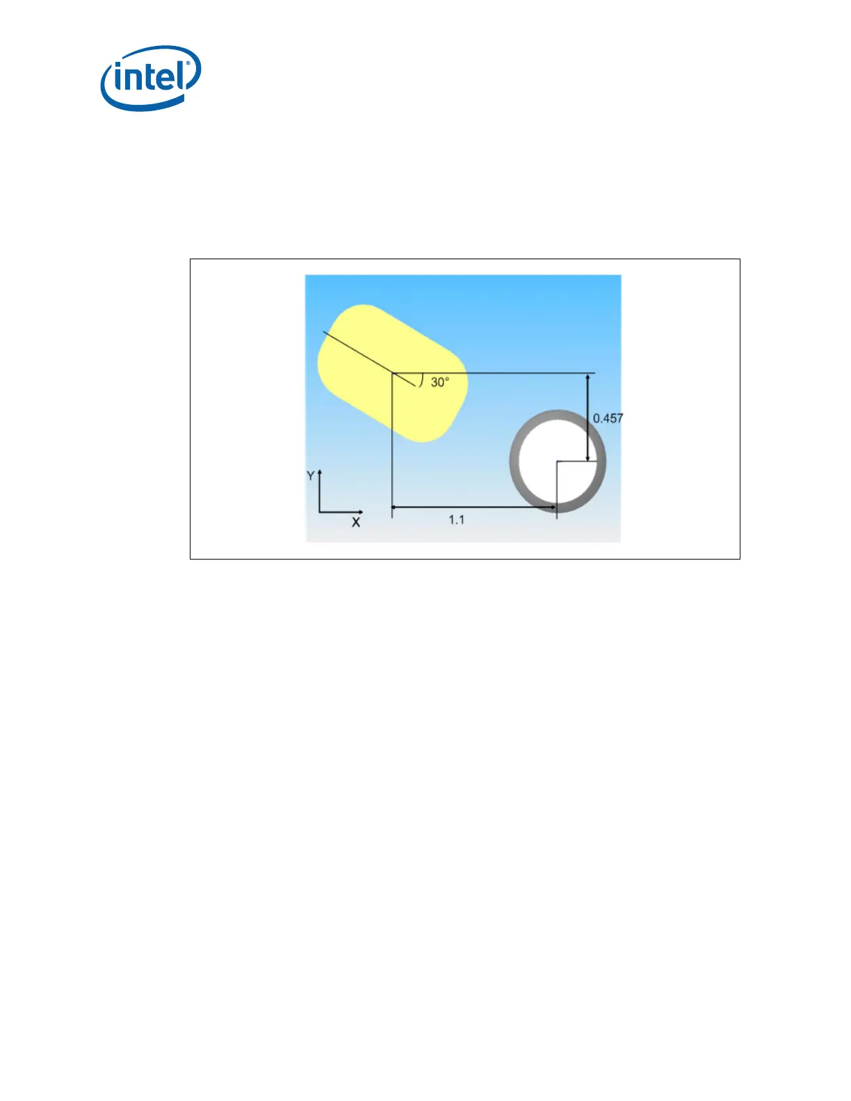
All socket contacts are designed such that the contact tip lands within the substrate pad
boundary before any actuation load is applied and remain within the pad boundary at
final installation, after actuation load is applied. The offset between LGA land center
and solder ball center is defined in Figure 3-5.
Note: All dimensions are in mm.
3.2 Board Layout
The land pattern for the LGA2011-0 socket is 40 mils hexagonal array. For CTF (Critical
to Function) joints, the pad size will primarily be a circular Metal Defined (MD) pad and
these pads should be designated as a Critical Dimension to the PCB vendors with a
17 mil ±1 mil tolerance. Some CTF pads will have a SMD Pad (20 x 17 mil).
Note: There is no round-off (conversion) error between socket pitch (1.016 mm) and board
pitch (40 mil) as these values are equivalent.
Figure 3-5. Offset between LGA Land Center and Solder Ball Center