XGB Analog edition manual
2 - 28
2.12 Configuration and Function of Internal Memory
A/D conversion module has the internal memory to transmit/receive data to/from PLC CPU.
2.12.1 I/O area of A/D converted data
I/O area of A/D converted data is as displayed in table.
Device assigned
(“S” or “H” type)
Device assigned
(IEC type)
Details R/W Sign direction
UXY.00.0
UXY.00.F
%UX0.x.0
%UX0.x.15
Module ERROR flag
Module READY flag
R
A/D
→ CPU
UXY.01.0
UXY.01.1
UXY.01.2
UXY.01.3
%UX0.x.16
%UX0.x.17
%UX0.x.18
%UX0.x.19
CH0 Run flag
CH1 Run flag
CH2 Run flag
CH3 Run flag
R A/D
→ CPU
UXY.02
%UW0.x.2
Ch0 digital output value R
A/D
→ CPU
UXY.03
%UW0.x.3
Ch1 digital output value R
UXY.04
%UW0.x.4
Ch2 digital output value R
UXY.05
%UW0.x.5
Ch3 digital output value R
UXY.11.0
%UX0.x.176
Flag to request error clear W CPU → A/D
- In the device assigned, X stands for the Base No. and Y for the Slot No. on which module is installed.
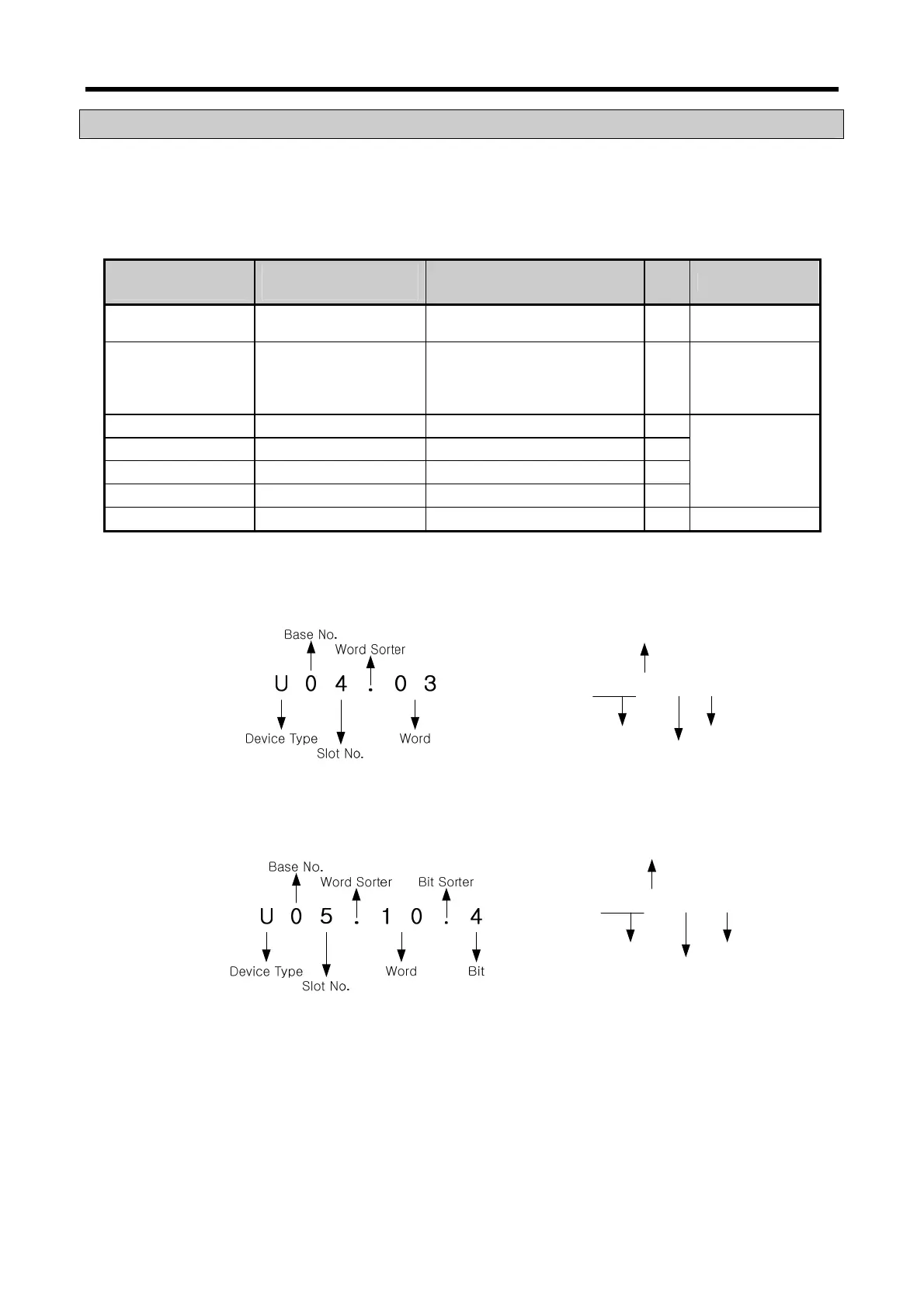
- In order to read ‘CH1 digital output value’ of A/D conversion module installed on Base No.0, Slot No.4,
it shall be displayed as U04.03. (in case of IEC type, %UW0.4.3)
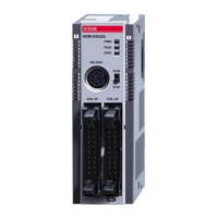
- In order to read ‘Flag to detect CH4 disconnection’ of A/D conversion module installed on Base No.0,
Slot No.5, it shall be displayed as U05.10.4.
Device Type
% U W 0 . 4 . 3
Slot No.
Base No
Word
“S” or “H” type
IEC type
“S” or “H” type
Device Type
% U X 0 . 5 . 19
Slot No.
Base No
Bit
IEC type