Chap. 6 Analog I/O Module (XBF-AH04A)
6.11 Constitution and Function of Internal Memory
An analog I/O module has internal memory for data communication with XGB base unit.
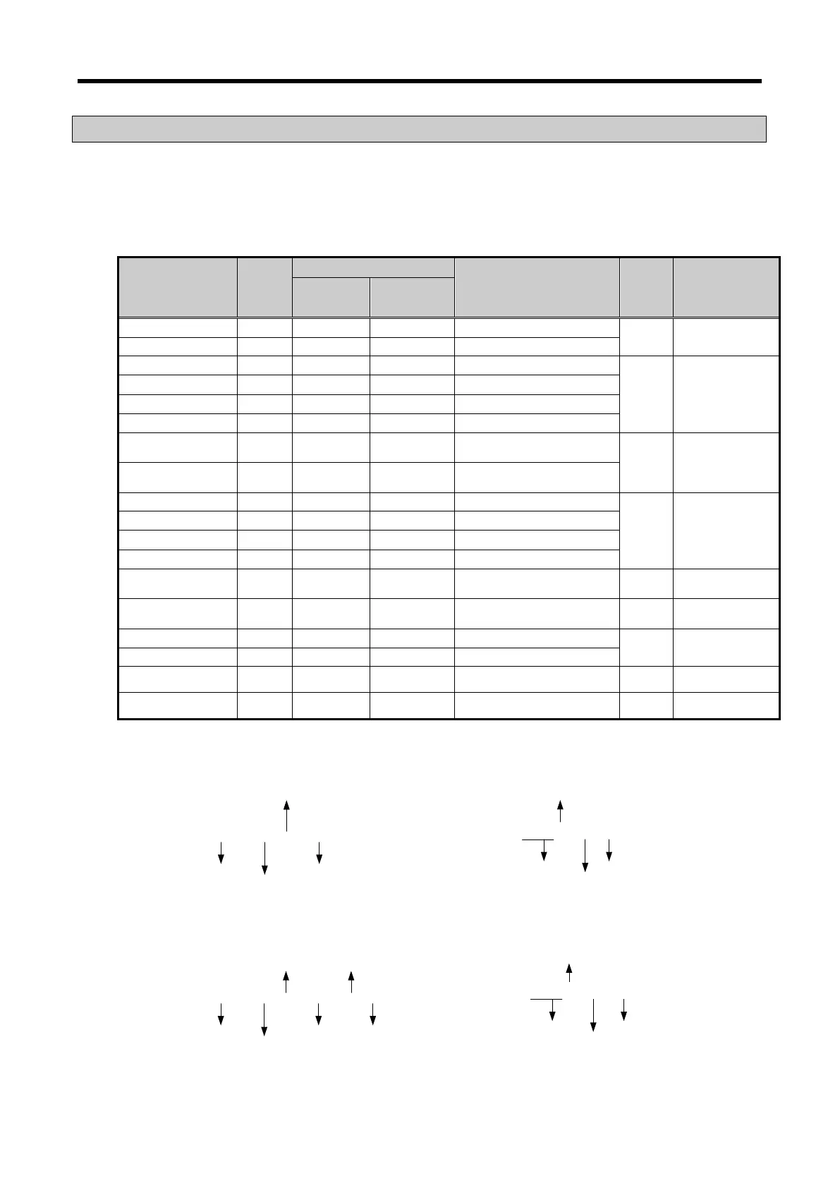
6.11.1 Analog Data I/O Area
The table below presents the analog data I/O area.
Variable Type
Description
Read/
Write
Signal
Direction
“S” or “H”
Type
IEC Type
Read AH04A → CPU
Read
AH04A → CPU
_0y_AD0_IDD BIT U0y.01.4 %UX0.y.20
Input Ch 0 open wire
detected
Read
AH04A → CPU
_0y_AD1_IDD BIT U0y.01.5 %UX0.y.21
Input Ch 1 open wire
detected
Read
AH04A → CPU
_0y_DA0_ERR
BIT
U0y.01.A
%UX0.y.26
Output Ch 0 error
_0y_AD0_DATA WORD U0y.04 %UW0.y.4
Input Ch 0 converted
value
Read
AH04A → CPU
_0y_AD1_DATA WORD U0y.05 %UW0.y.5
Input Ch 1 converted
value
AH04A → CPU
Ch 0 output state setting
Write AH04A ↔ CPU
Ch 1 output state setting
_0y_DA0_DATA WORD U0y.07 %UW0.y.7 Output Ch 0 input value
AH04A ↔ CPU
_0y_DA1_DATA WORD U0y.08 %UW0.y.8 Output Ch 1 input value
AH04A ↔ CPU
- In the device allocation, the small letter ‘y’ is the No. of the slot where the module is installed.
- For example, to read the ‘Input Ch 1 Converted Value’ of the analog I/O module installed in the
4
th
slot, write in U04.05. (%UW0.4.5 for IEC types)
Device Type
U 0 4 . 0 5
Slot No.
Word
[“S”or“H”type]
Word classifier
Device Type
Slot No.
Base No
Word
[IEC type]
% U W 0 . 4 . 5
- To read the ‘Output Ch 1 Output Status Setting’ of the analog I/O module installed in the 5
th
slot,
write in U05.06.1 (%UX0.5.97 for IEC types)
Device Type
U 0 5 . 0 6
Slot No.
Word classifier
Word
. 1
Bit classifier
[“S”or“H”type]
Device Type
% U X 0 . 5 . 97
Slot No.
Base No
[IEC type]
6 - 33